In a groundbreaking development that sheds new light on the intricate world of quantum materials, a collaborative research team has achieved the unprecedented feat of directly visualizing how the strength and spatial coherence of electronic order evolve during a phase transition. This breakthrough, led by Professor Yongsoo Yang of the Department of Physics at the Korea Advanced Institute of Science and Technology (KAIST) in conjunction with Professors SungBin Lee, Heejun Yang, and Yeongkwan Kim, and collaborators at Stanford University, marks a significant advance in the long-standing quest to understand charge density waves (CDWs) – a fundamental form of electronic organization in many exotic materials. Their findings, published in Physical Review Letters, provide a new experimental framework for exploring the complex interplay of electronic and structural factors that govern these fascinating quantum states.
Unraveling the Mysteries of Electronic Order in Quantum Materials
Quantum materials are a class of substances where the collective behavior of electrons gives rise to extraordinary properties, such as superconductivity, colossal magnetoresistance, or topological states. Unlike conventional materials where electrons often behave as independent particles, in quantum materials, strong interactions between electrons and the underlying crystal lattice lead to complex emergent phenomena. One such phenomenon is the formation of electronic order, where electrons spontaneously arrange themselves into intricate patterns. This order rarely forms in a smooth, uniform manner; instead, it frequently appears as complex, spatially varying textures.
Among the most well-known examples of electronic order is the charge density wave (CDW). A CDW is a state where electrons, often at low temperatures, organize into a repeating, periodic pattern of charge density, much like a standing wave. This periodic modulation of electron density is accompanied by a subtle distortion of the crystal lattice, as the atomic nuclei adjust to the new electronic configuration. First theorized in the 1930s and experimentally confirmed in the 1970s, CDWs have been a subject of intense research for decades due to their fundamental role in many quantum systems. They can act as precursors to superconductivity, compete with other electronic orders, and offer insights into the delicate balance of forces within a material. Despite extensive study using techniques like X-ray diffraction, which provides an average picture of the order across a macroscopic sample, and scanning tunneling microscopy (STM), which offers surface-sensitive information, directly observing how the amplitude (strength) and spatial coherence (how well-connected the pattern is) of a CDW evolve across space and temperature, especially during a phase transition, has remained a significant experimental challenge.
Traditional methods often provide an averaged signal over a large area, obscuring the local variations crucial for understanding complex phase transitions. The precise mechanisms by which CDWs form, grow, weaken, and ultimately break apart as external parameters like temperature are changed have thus largely been inferred indirectly, leaving a critical gap in our understanding of these foundational quantum phenomena. This knowledge gap has hindered efforts to precisely control and manipulate the properties of quantum materials for potential technological applications.
A Breakthrough in Nanoscale Imaging: The Power of 4D-STEM
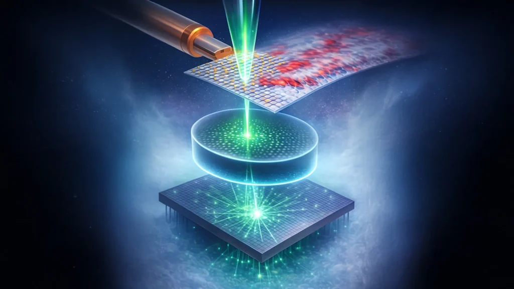
To overcome these long-standing observational limitations, the KAIST and Stanford team employed an advanced experimental setup centered around a liquid-helium-cooled electron microscope integrated with four-dimensional scanning transmission electron microscopy (4D-STEM). This cutting-edge combination allowed them to peer into the atomic and electronic structure of quantum materials with unprecedented detail and precision.
The choice of instrumentation was critical. First, the liquid-helium-cooled stage is essential for reaching the extremely low temperatures—as cold as -253°C (approximately 20 Kelvin)—where many quantum phenomena, including CDWs, emerge and become stable. At these cryogenic temperatures, thermal fluctuations are minimized, allowing the subtle quantum effects to dominate. Second, 4D-STEM is a revolutionary technique that goes beyond conventional electron microscopy. In traditional STEM, a focused electron beam scans across a sample, and detectors collect information about the scattered electrons. 4D-STEM, however, captures a full two-dimensional diffraction pattern at every single pixel as the electron beam scans. This results in a four-dimensional dataset (two spatial dimensions from the scan, and two momentum-space dimensions from the diffraction pattern), providing a rich tapestry of information about both the real-space atomic arrangement and the momentum-space electronic order.
By analyzing these detailed diffraction patterns, the researchers could precisely extract information about the periodicity, strength (amplitude), and orientation of the CDW at each point in the material. This enabled them to create detailed nanoscale maps that not only indicated the presence of electronic order but, crucially, quantified its strength and tracked its connections across different regions of the sample. The spatial resolution achieved by their microscope was truly remarkable, capable of resolving structures as small as one hundred-thousandth the width of a human hair – a scale where individual electron patterns and lattice distortions become visible.
The process can be aptly compared to observing the formation of ice crystals as water freezes, but under an unimaginably powerful microscope. Instead of water molecules, the team observed electrons arranging themselves into intricate patterns. This ability to directly map the CDW amplitude and its spatial coherence as temperature changed allowed them to visualize the dynamic evolution of electronic order across a phase transition in a way that was previously impossible. This direct approach offers a significant advantage over indirect inference methods, providing definitive, spatially resolved evidence of how electronic order manifests and transforms within a material.
Revealing Patchy Patterns and the Influence of Strain
The high-resolution 4D-STEM imaging unveiled several surprising and highly significant findings that challenge previous assumptions about electronic order. One of the most striking observations was that electronic order does not spread evenly throughout the material. Instead, the nanoscale maps revealed a heterogeneous landscape where CDW order formed in "scattered patches." Some areas exhibited clear, well-defined, and strong CDW patterns, while adjacent regions showed little to no electronic order. This phenomenon was vividly described by the researchers as resembling a lake where ice forms in isolated patches rather than uniformly covering the entire surface. This patchy formation indicates that local conditions play a much more critical role in the nucleation and growth of electronic order than previously understood, suggesting a high degree of spatial inhomogeneity in quantum material properties.
Another pivotal discovery concerned the profound influence of subtle structural imperfections. The study found a strong and direct link between these uneven electronic patterns and minute distortions within the crystal lattice, known as strain. Even "minute amounts of strain"—distortions far too small to be detected by conventional optical methods or even many other advanced characterization techniques—were sufficient to significantly weaken the CDW amplitude in those regions. This provides compelling direct evidence that subtle lattice distortions are not merely passive bystanders but active participants, playing a crucial role in shaping how these electronic patterns form and evolve. This electron-lattice coupling, where the electrons influence the lattice and vice-versa, is a hallmark of many quantum materials, and this study offers an unprecedented nanoscale view of its direct impact. The ability to spatially correlate strain with CDW amplitude opens new avenues for understanding and potentially controlling these interactions.
Challenging Conventional Phase Transition Understanding
The research also yielded a surprising insight into the nature of phase transitions in quantum materials. It was discovered that small pockets of CDW order could persist even above the material’s nominal transition temperature, a point where long-range order is conventionally expected to vanish entirely. This finding suggests that the phase transition from an ordered state to a disordered state is not a simple, uniform process where order abruptly disappears across the entire material. Instead, the electronic order gradually loses its spatial coherence, with local regions retaining some degree of order even as the macroscopic, long-range order dissipates. This "precursor" behavior above the transition temperature highlights the complex, multi-stage nature of phase transitions in correlated electron systems and offers a more nuanced picture than previously available. It implies that localized fluctuations and remnants of order can exist in a broader temperature range than previously thought, influencing the material’s properties even in the "disordered" phase.
A key technical and conceptual achievement of this work was the first direct measurement of correlations in CDW amplitude. By meticulously examining how the strength of electronic order at one location related to that at another, the researchers were able to quantify how coherence breaks down across the phase transition while local amplitude might still be present. This level of detail, inaccessible through traditional techniques like diffraction (which averages over vast areas) or scanning probe methods (which often lack the momentum-space information needed to fully characterize collective order), provides an invaluable new metric for characterizing the evolution of quantum phases. It offers a powerful tool to distinguish between a complete collapse of order and a mere loss of its spatial connectivity.
A New Framework for Future Quantum Material Research
The implications of this study extend far beyond the specific charge density wave material investigated. Charge density waves are a fundamental feature of many quantum materials and frequently interact with other electronic states, including superconductivity, magnetism, and topological phases. By directly mapping their spatial structure and correlations at the nanoscale, this research provides a powerful new experimental approach for understanding how collective electronic order forms, evolves, and interacts in real systems.
Professor Yongsoo Yang underscored the transformative nature of these findings: "Until now, the spatial coherence of charge density waves was largely inferred indirectly, leaving much to speculation about their true local behavior. Our approach allows us to directly visualize how electronic order varies across space and temperature, and, critically, to identify the factors—such as local strain—that locally stabilize or suppress it. This is a game-changer for understanding the microscopic mechanisms governing these complex materials." This direct visualization capability moves the field beyond indirect inference, providing concrete, spatially resolved evidence.
The ability to precisely map the amplitude and spatial coherence of CDWs opens up numerous avenues for future research. Scientists can now investigate how different types of defects, boundaries, or engineered strain fields might be used to control or enhance specific electronic orders. This could have profound implications for the design of new quantum devices, where local control over electronic properties is paramount. For instance, understanding how strain can weaken CDWs might enable researchers to engineer materials to suppress unwanted CDW states that compete with superconductivity, potentially leading to higher-temperature superconductors. Conversely, in applications where CDW order is desired, this knowledge could guide strategies to stabilize and enhance it.
The collaborative nature of the research, involving contributions from Seokjo Hong, Jaewhan Oh, and Jemin Park of KAIST as co-first authors, alongside the expertise from Stanford University, highlights the interdisciplinary effort required to tackle such complex problems in condensed matter physics. The research was primarily supported by substantial grants from the National Research Foundation of Korea (NRF), including the Individual Basic Research Program, Basic Research Laboratory Program, and Nanomaterial Technology Development Program, funded by the Korean Government (MSIT). Additional support came from the KAIST singularity professor program, the Nano Material Technology Development Program, and the Korea Research Institute of Standards and Science (KRISS), acknowledging the significant investment in advanced scientific infrastructure and talent. The use of state-of-the-art equipment, including double Cs corrected Titan cubed G2 60-300 and Spectra Ultra instruments at the KAIST Analysis Center for Research Advancement (KARA), underscores the technical sophistication behind this groundbreaking work.
In essence, this study provides an unprecedented microscopic lens through which to observe the dynamic choreography of electrons in quantum materials. By offering a direct window into the nanoscale world of charge density waves, it lays a robust foundation for future explorations into the fundamental physics of electronic order, potentially accelerating the discovery and development of new materials with revolutionary functionalities.