The challenge of expanding input capabilities without migrating to larger, more expensive chips has led to the development of several multiplexing techniques. However, many traditional methods introduce their own sets of compromises, ranging from excessive software overhead to the requirement of additional integrated circuits (ICs). Recent developments in analog-to-digital converter (ADC) utilization have paved the way for more efficient solutions, allowing for the detection of multiple simultaneous button presses using a minimal number of pins while maintaining high noise immunity.
The Evolution of Input Management in Embedded Systems
Historically, the most straightforward method for connecting switches to a microcontroller was the direct connection: one pin per switch. While simple to implement, this approach is the least efficient in terms of resource allocation. As complexity grew, developers turned to matrix scanning, a technique that arranges switches in rows and columns. A 4×4 matrix, for instance, allows for 16 inputs using only 8 GPIO pins. While a significant improvement, matrices still require a relatively high pin count for small-scale projects and often necessitate the use of diodes to prevent "ghosting"—a phenomenon where multiple simultaneous presses create parasitic paths that lead to incorrect input detection.
For systems where pin counts are extremely restricted, digital communication protocols like I2C (Inter-Integrated Circuit) became the standard. By using a dedicated port expander chip, such as the PCF8574 or MCP23017, a designer can gain 8 to 16 additional GPIO pins while consuming only two pins on the host microcontroller (SDA and SCL). However, this solution introduces a "silicon tax." Not only does it require an additional physical component, increasing the Bill of Materials (BOM) cost and PCB footprint, but it also demands significant software resources. On microcontrollers with limited flash memory, such as those with 1kB or 2kB capacities, the inclusion of an I2C library can consume a disproportionate amount of available space. For example, implementing a software-based I2C routine to read a port expander can require upwards of 190 bytes of flash memory, a heavy burden for ultra-lightweight applications.
Analyzing the Constraints of Shift Registers and Charlieplexing
Shift registers, such as the 74HC165 for inputs or the 74HC595 for outputs, offer another alternative. These chips are faster than I2C expanders and require less complex software, as they rely on a simple bit-shifting mechanism. A standard implementation requires three pins (Data, Clock, and Latch), though creative engineering can reduce this to two or even a single pin using RC-delay elements. Despite these advantages, shift registers remain rigid; they are typically unidirectional, meaning a single chip cannot mix inputs and outputs. Furthermore, like I2C expanders, they necessitate an additional IC, which may be unacceptable in space-constrained handheld devices.
Charlieplexing, a technique famously used to drive large arrays of LEDs with minimal pins, can also be adapted for inputs. Using the tri-state logic of microcontroller pins (High, Low, and High-Z/Input), Charlieplexing follows the formula $n(n-1)$ for the number of inputs supported by $n$ pins. While mathematically impressive—allowing 6 switches on 3 pins—it is rarely used for inputs because it cannot reliably detect simultaneous button presses and requires a diode for every switch, complicating the hardware assembly.

The Analog Shift: Leveraging the Resistive Ladder
When a microcontroller features an integrated Analog-to-Digital Converter (ADC), the paradigm shifts from digital logic to voltage division. By associating different switches with specific voltage levels, a single analog pin can theoretically service dozens of inputs. The most common implementation is the resistive ladder, where switches are connected to a voltage divider.
In a standard parallel resistive ladder, pressing a button alters the total resistance of the network, thereby changing the voltage seen by the ADC. While this saves pins, it introduces non-linearity. The gaps between detectable voltage levels become progressively smaller as more resistors are added in parallel, leading to a precarious noise margin. In a 3-switch configuration using standard E12 series resistors, the smallest gap between states can be as low as 59mV. In environments with electrical noise or power supply fluctuations, this narrow margin can lead to "jitter" or false triggers. Furthermore, decoding these non-linear values in software requires a series of complex IF-ELSE statements, which, while functional, consumes more flash memory than a linear solution.
A Novel Approach to Resistive Multiplexing
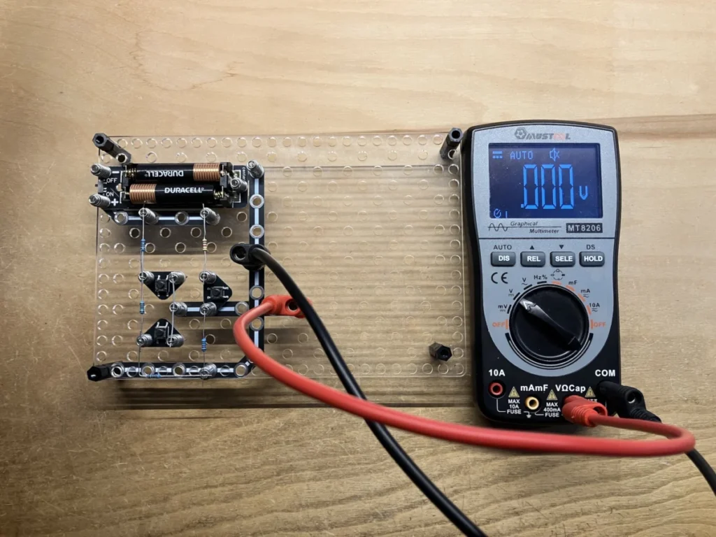
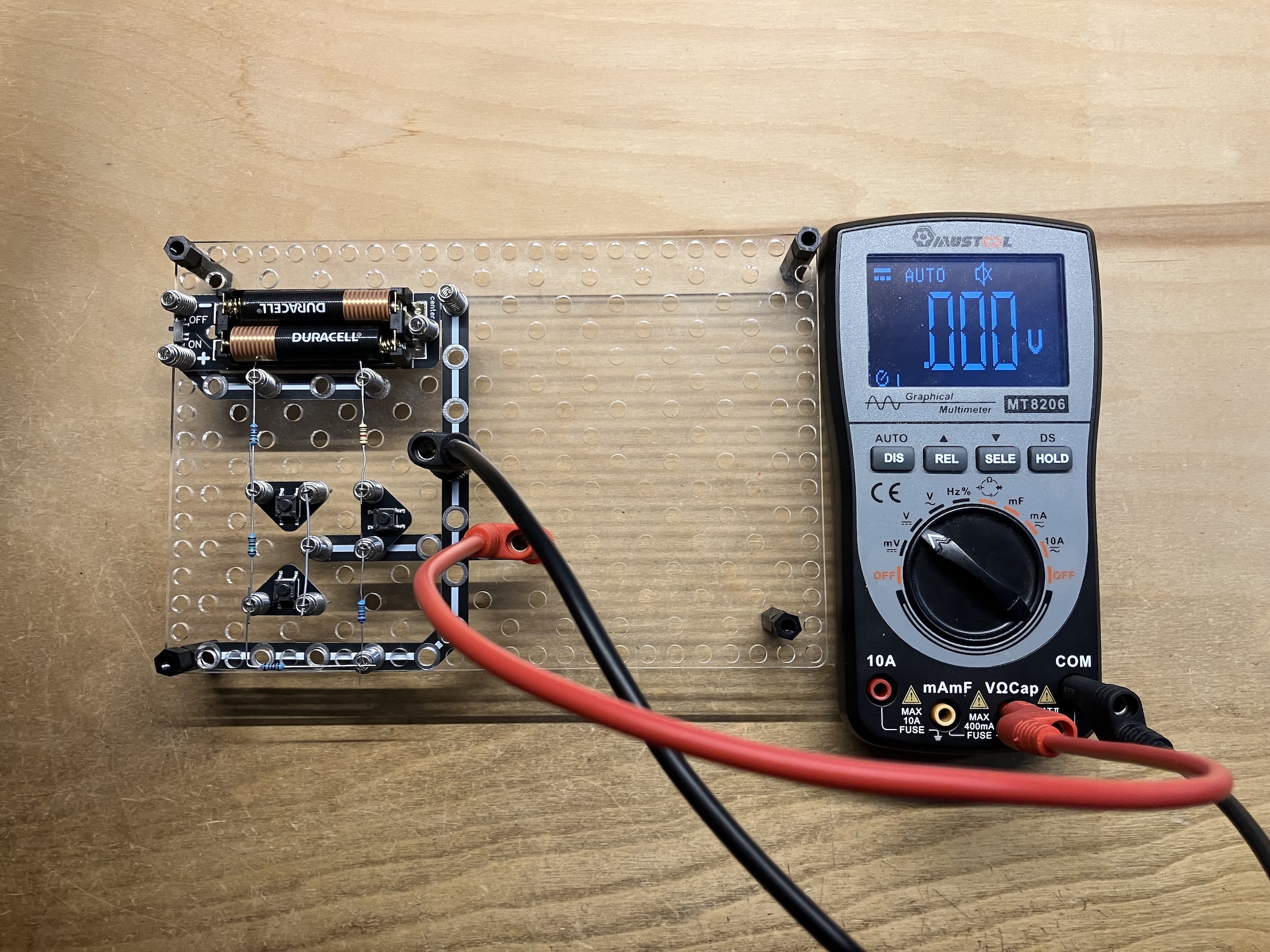
To address the limitations of standard resistive ladders, a new 5-resistor configuration has been proposed that optimizes both noise margins and software efficiency. This novel solution focuses on changing the resistances on both sides of the voltage divider simultaneously. By carefully selecting resistor values from the E12 series, this configuration produces much more uniform voltage intervals between different switch states.

In this improved model, the system can distinguish between seven distinct states: no buttons pressed, three individual button presses, and the three possible combinations of two simultaneous button presses. This is particularly vital for handheld D-pads, where diagonal movement is achieved by pressing two adjacent buttons (e.g., Up and Right).
Data analysis of this novel resistive solution shows a significant performance leap:
- Noise Margin: The worst-case noise margin increases from 59mV to 124mV, more than doubling the reliability of the system.
- Flash Memory Footprint: Because the voltage levels are more uniformly distributed, the decoding logic is simplified. The routine requires approximately 94 bytes of flash memory, compared to 162 bytes for a standard ladder and 190 bytes for an I2C solution.
- Decoding Efficiency: By assuming a 10-bit ADC and a 3V power supply, the three most significant bits (MSB) of the ADC value can be used to identify the switch state. Shifting the ADC value right by 7 bits and using a small 8-byte lookup table allows for nearly instantaneous input identification with minimal CPU cycles.
The Diode Ladder: Achieving Binary-Weighted Precision
For applications where software simplicity is the absolute priority, the "Diode Ladder" offers a compelling, albeit environmentally sensitive, alternative. This method utilizes the forward voltage drops of different types of diodes to create a binary-weighted voltage output.

By using a combination of Schottky diodes (with a forward voltage of roughly 0.37V) and silicon diodes (such as the 1N4148 with a drop of 0.7V), designers can create a ladder where the ADC output directly corresponds to the binary state of the switches. In this setup, the 3 most significant bits of the ADC value map directly to the switch positions, eliminating the need for complex lookup tables or interval comparisons.
However, the diode ladder introduces a significant engineering trade-off: temperature sensitivity. Diode forward voltage typically drifts by -2mV/°C. In a device intended for outdoor use or industrial environments with wide temperature swings, this drift could cause the voltage levels to shift into the wrong "bins," resulting in incorrect input detection. To mitigate this, engineers may incorporate a Negative Temperature Coefficient (NTC) resistor into the circuit to compensate for the drift, though this adds complexity and cost back into the system.
Broader Implications for Industrial and Maker Design
The refinement of these multiplexing techniques reflects a broader trend in the electronics industry toward "extreme optimization." As the Internet of Things (IoT) expands, there is an increasing demand for "disposable" or ultra-low-cost smart devices. In these applications, the difference of a few cents in BOM cost or a few dozen bytes in code size can determine the commercial viability of a product.

For the maker community, these techniques democratize the use of low-end hardware. Being able to squeeze a full user interface out of an ATtiny85 or a similar 8-pin microcontroller allows for the creation of smaller, more efficient wearable tech and handheld gadgets. The ability to detect simultaneous presses—a feature often lost in cheap multiplexing schemes—ensures that user experience is not sacrificed for the sake of hardware economy.
Conclusion and Future Outlook
The choice between I2C expanders, shift registers, matrices, and advanced analog ladders ultimately depends on the specific requirements of the project. If high pin counts (16+) are required and flash memory is abundant, I2C remains the gold standard. However, for the vast majority of small-scale embedded projects where only a few extra pins are needed, the novel resistive solution provides the most balanced approach. It offers high noise immunity, supports simultaneous presses, and maintains an exceptionally small software footprint.
As microcontroller architectures continue to integrate more capable ADCs even in their smallest packages, the shift toward analog-based input multiplexing is likely to accelerate. The engineering challenge remains the same: achieving maximum functionality with minimal resources. Through creative circuit design and a deep understanding of component characteristics, developers can continue to push the boundaries of what is possible with even the most modest silicon.