Scientists at Monash University have unveiled a pioneering integrated circuit capable of generating, directing, and reading information carried by light, all within a single, tiny chip. This significant advancement addresses a long-standing challenge in the burgeoning field of "valleytronics," promising profound implications for the future of computing, energy efficiency, and quantum technologies. The breakthrough, detailed in the prestigious journal Nature Photonics, marks a pivotal moment, showcasing a fully integrated system that operates efficiently at room temperature, overcoming a major hurdle for many emerging quantum technologies.
Unpacking the Promise of Valleytronics
To fully appreciate the significance of this Monash innovation, it is essential to understand the realm of valleytronics. For decades, conventional electronics have relied on the flow of electrons and their charge to process information. More recently, "spintronics" emerged, leveraging the spin of electrons as an additional property to encode data, offering potential improvements in speed and energy efficiency. Valleytronics represents an even newer frontier, utilizing a quantum property known as the "valley degree of freedom."
In certain two-dimensional materials, electrons can exist in distinct energy minima, or "valleys," within their band structure. These valleys are characterized by specific momentum states. The valley degree of freedom refers to the ability to manipulate and utilize the electron’s presence in one valley or another as a binary information carrier – akin to a 0 or 1 in traditional computing. This property offers a unique pathway for encoding, transmitting, and processing data with potentially unprecedented efficiency and speed. Unlike charge-based electronics, which suffer from significant energy loss through heat dissipation, and spintronics, which can be susceptible to decoherence, valleytronics holds the promise of ultralow-power operation and robust information encoding. The concept suggests the possibility of building logic gates and memory devices that operate on valley states, leading to a new generation of information technologies. However, a primary obstacle has been the difficulty in efficiently generating, manipulating, and detecting these valley states on a single, integrated platform.
A Fully Integrated Solution: The Monash Breakthrough
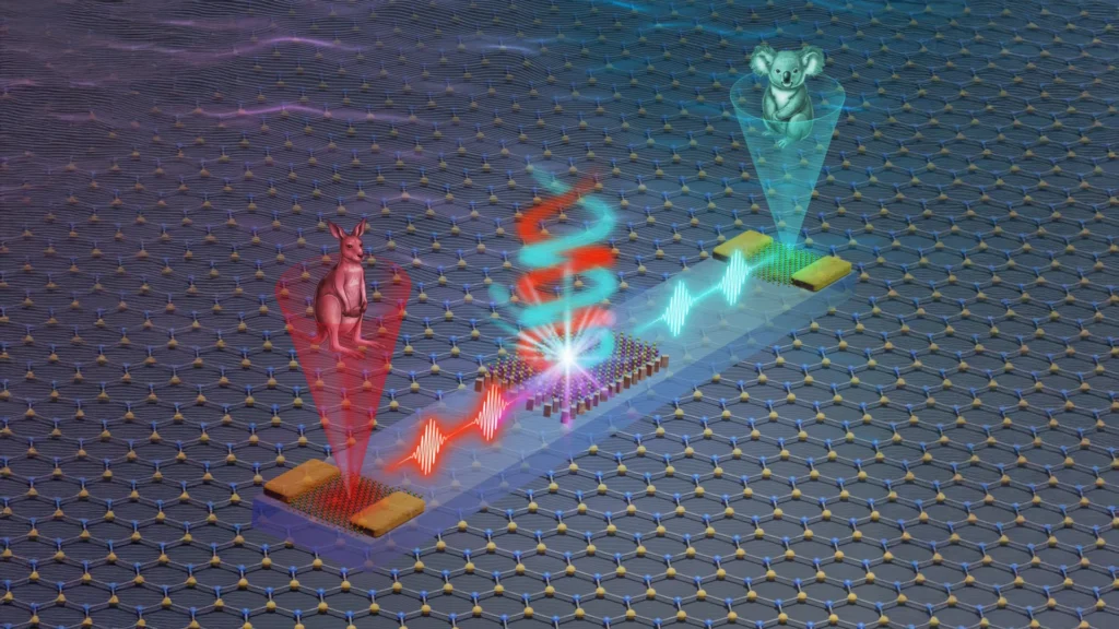
The Monash University team, primarily from the School of Physics and Astronomy, has successfully engineered a device that tackles this integration challenge head-on. Their new chip is the first of its kind to combine all three crucial functions of valleytronics: generating specialized light signals that encode valley information, steering these signals along specific paths, and converting them back into electrical signals, all within the same compact system. This achievement is a leap forward from previous research, where scientists could either generate valley-polarized light or detect it, but not seamlessly integrate both functions with precise control on a single chip.
Lead author Dr. Chi Li, whose team’s findings were published in Nature Photonics, emphasized the comprehensive nature of their system. "Until now, we could generate or detect these signals, but not do everything in one integrated device," Dr. Li stated. "What we’ve built is a complete on-chip system that can create, route and read this information with very high precision." This precision is paramount for reliable data encoding and transmission, distinguishing this development from prior fragmented approaches. The ability to precisely control the propagation and conversion of valley-encoded light signals opens up possibilities for complex computational architectures that were previously theoretical.
Engineering Excellence: Materials and Nanostructures
The innovation hinges on a sophisticated blend of advanced nanotechnology and cutting-edge materials. At the heart of the device are ultra-thin materials, typically just a few atoms thick. These are often transition metal dichalcogenides (TMDs), a class of 2D materials like molybdenum disulfide (MoS2) or tungsten diselenide (WSe2), which possess unique optical and electronic properties suitable for valleytronic applications. Specifically, TMDs exhibit strong light-matter interaction and can emit light with specific polarization depending on the valley state of the excited electrons, making them ideal for generating valley-polarized light.
These atomically thin materials are meticulously paired with specially engineered nanostructures, known as metasurfaces. Metasurfaces are subwavelength-structured interfaces designed to precisely control light at extremely small scales, manipulating its amplitude, phase, and polarization. In this context, the metasurfaces are crucial for both directing the valley-encoded light signals along specific pathways on the chip and for efficiently converting these optical signals into detectable electrical currents.
Dr. Kaijian Xing, co-first author of the study and a Research Fellow at Monash University, detailed the practical methodology behind this integration. "We employ a straightforward stacking approach to integrate ultra-thin materials with metasurfaces, overcoming the technical challenges of direct material growth on photonic structures, and enabling further advances in valleytronics," Dr. Xing explained. Direct growth of 2D materials onto complex photonic structures is often fraught with issues related to material quality and interface defects. The stacking approach offers a more scalable and reliable pathway, facilitating the fabrication of high-performance integrated valleytronic devices. This ingenious engineering solution sidesteps significant manufacturing hurdles, accelerating the potential for practical applications.
Room Temperature Operation: A Quantum Leap for Practicality
One of the most profound advantages of this new technology is its ability to operate effectively at room temperature. Many cutting-edge quantum systems, particularly those involved in quantum computing and certain advanced sensing applications, demand extremely cold, cryogenic environments – often requiring temperatures close to absolute zero (-273.15 °C). Maintaining such ultra-low temperatures necessitates complex, bulky, and energy-intensive refrigeration systems, making these technologies difficult, expensive, and impractical for widespread use outside of specialized laboratories.
The Monash chip’s room-temperature functionality represents a significant leap towards real-world applicability. It drastically reduces the cost, complexity, and physical footprint associated with implementing valleytronic technologies. This inherent practicality positions the technology for faster adoption in commercial and industrial settings, removing a major barrier that has historically slowed the transition of quantum-inspired research from the lab to market.
Senior author Dr. Haoran Ren, an ARC Future Fellow and leader of the Monash NanoMeta Group, underscored this critical advantage. "This is a significant step toward scalable, chip-based technologies that use light instead of electricity to process information," Dr. Ren stated. He highlighted that the work could pave the way for a new generation of compact photonic devices that are both highly programmable and remarkably efficient, fundamentally changing how data is handled in future systems.
Demonstrating Capabilities: Processing Multiple Data Streams
To validate the chip’s robust capabilities, the Monash researchers conducted a compelling demonstration: they successfully encoded and processed two separate images simultaneously. This experiment showcased the device’s ability to manage multiple streams of information concurrently, a crucial feature for future computing architectures that demand parallel processing capabilities to handle ever-increasing data volumes.
This parallel processing capability is central to enhancing computational speed and efficiency. In conventional computing, bottlenecks often arise from sequential data processing. By leveraging the unique properties of light and valley states, the Monash chip demonstrates a pathway towards true multiplexing, where different channels of information can be processed independently and simultaneously on the same device. This has direct implications for applications requiring high-throughput data processing, such as advanced imaging, artificial intelligence, and complex simulations.
Broader Impact and Future Horizons
The implications of the Monash University team’s breakthrough extend across several critical technological domains:
Faster Computing: Photonic devices, by their very nature, utilize light, which travels significantly faster than electrons in electronic circuits. This enables ultra-fast data transmission speeds, potentially pushing the boundaries of computational throughput beyond the limits of current silicon-based technologies. The integration of valleytronics further enhances this by providing an additional degree of freedom for encoding data, allowing more information to be carried per photon.
Lower Energy Consumption: One of the most pressing challenges in modern computing is the escalating energy consumption of data centers and personal devices, largely due to the heat generated by electrical resistance. Photonic devices inherently generate less heat, leading to substantially lower energy consumption. This has profound environmental and economic benefits, contributing to more sustainable computing infrastructure.
Quantum Technologies: The manipulation of quantum properties like the valley degree of freedom is fundamental to quantum information science. This chip could serve as a foundational component for various quantum technologies, including quantum computing where valley states could act as robust qubits or assist in quantum communication by enabling novel methods for secure data transmission through quantum cryptography.
Advanced Imaging: The ability to precisely control and detect light signals, especially those carrying rich quantum information, could lead to significant advancements in imaging technologies. This might include ultra-high-resolution imaging, non-invasive biological imaging, or even quantum imaging techniques that surpass classical limits.
Next-Generation Optical Communication Systems: With massive bandwidths and ultra-fast data transmission speeds, the technology holds strong potential for revolutionizing optical communication. This could lead to vastly improved internet speeds, more efficient data transfer between computing nodes, and a more robust global communication infrastructure.
Professor Stefan A. Maier, Head of the School of Physics and Astronomy and Nanophotonics Laboratory at Monash University, highlighted the broader significance of the development. "This is an important step toward fully integrated valleytronic systems," said Professor Maier. "By combining light and quantum materials on a chip, we can access new ways of encoding and processing information." His statement underscores the bridging of fundamental scientific discoveries with practical, scalable technological applications, a hallmark of impactful research.
A Global Collaborative Effort
This pioneering research was the result of a truly international collaboration, bringing together diverse expertise from across the globe. The project involved researchers from Australia, China, Singapore, Germany, and Japan, demonstrating the power of intercontinental scientific synergy in tackling complex challenges. This multinational effort combined specialized knowledge in nanophotonics, the study of light-matter interactions at the nanoscale; two-dimensional materials, which are critical for the valleytronic effect; and optoelectronics, the application of electronic devices that source, detect, and control light.
The core Monash University team included Dr. Chi Li, Dr. Kaijian Xing, Professor Michael S. Fuhrer, Professor Stefan A. Maier, and Dr. Haoran Ren. Their contributions were augmented by significant input from other prestigious institutions, including the Singapore University of Technology and Design, LMU Munich, and the University of Technology Sydney. Such collaborations are increasingly vital in modern scientific discovery, pooling resources, knowledge, and perspectives to accelerate breakthroughs that would be far more challenging for any single institution to achieve alone.
Outlook and Future Directions
The Monash University breakthrough represents a significant validation of the valleytronics paradigm and its potential to revolutionize information technology. While the immediate focus is on further refining the chip’s performance and exploring its capabilities in more complex computational tasks, the long-term vision is clear: to integrate such devices into larger systems that can truly leverage the speed, energy efficiency, and quantum advantages offered by light and valley states.
The scientific community is likely to react with considerable enthusiasm to this development, as it addresses a fundamental roadblock in the path towards practical valleytronics. Industry stakeholders, particularly those in semiconductor manufacturing, telecommunications, and high-performance computing, will undoubtedly be watching closely. The prospect of room-temperature operation dramatically lowers the barrier to commercialization, making it a highly attractive area for future investment and development.
However, challenges remain. Scaling up the fabrication of these complex nanostructures and ultra-thin material stacks to mass production levels will require further engineering innovation. Integrating these new photonic-valleytronic components with existing electronic infrastructure also presents a significant hurdle. Nevertheless, the Monash team’s work provides a compelling blueprint and a robust proof-of-concept for the future of information processing. It pushes us closer to an era where information is not just processed by electrons, but by the subtle quantum dance of light and matter, paving the way for a new generation of compact, powerful, and sustainable computing and communication technologies.