The landscape of modern optics is undergoing a fundamental shift as researchers move away from the centuries-old reliance on bulky glass lenses toward a future defined by two-dimensional materials capable of manipulating light at the atomic level. A collaborative research effort led by the deep-tech company XPANCEO, in partnership with the National University of Singapore and the University of Chemistry and Technology, Prague, has announced a significant breakthrough in the study of molybdenum oxychloride (MoOCl2). This layered crystal has demonstrated unprecedented optical properties that could facilitate the development of "invisible" wearable technologies, including smart contact lenses and ultra-thin augmented reality (AR) glasses. The study, recently published in the prestigious journal Nano Letters, provides the first comprehensive experimental mapping of the crystal’s optical behavior, revealing that MoOCl2 possesses the strongest light-bending effect ever recorded in a natural material.
The Quest for Miniaturization in Optical Engineering
For decades, the primary constraint in the development of sophisticated optical devices has been the physical size of the components required to refract, reflect, and filter light. Traditional lenses operate on the principle of geometric optics, where the thickness and curvature of the material dictate how light is steered. This requirement has led to the "bulky" nature of current AR headsets and high-end camera systems. To achieve the goal of truly wearable, unobtrusive technology, scientists have turned their attention to nanophotonics and the study of anisotropic materials.
Anisotropy refers to the property of a material that allows it to change its physical characteristics based on the direction of the light or electrical current passing through it. While many crystals exhibit some degree of anisotropy, MoOCl2 represents an extreme case. The research team’s findings suggest that this material can perform the same light-manipulation tasks as traditional optics but at a fraction of the size. Specifically, these materials are thousands of times thinner than a human hair, offering a pathway to integrate complex optical circuits directly onto surfaces as thin as a contact lens.
A Material of Dual Identities: The Optical Chameleon
The research characterizes MoOCl2 as an "optical chameleon" due to its ability to oscillate between the properties of a metal and those of a dielectric (insulating) material like glass. This duality is rooted in the material’s unique atomic structure, which consists of one-dimensional chains of molybdenum atoms. Within these chains, electrons can move with relative ease, giving the material metallic properties along one axis. However, in the direction perpendicular to these chains, the material acts as a transparent insulator.
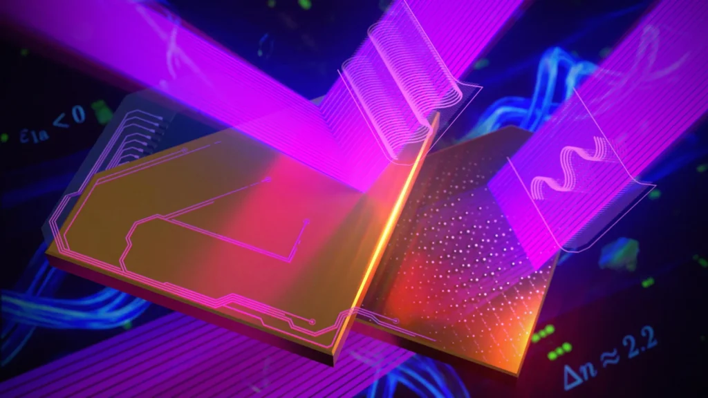
During experimental testing, the researchers observed that when the crystal is oriented in one direction, it reflects light with the efficiency of a polished metal surface. When rotated exactly 90 degrees, it becomes almost entirely transparent. This extreme variation is quantified by a property known as birefringence. The study recorded an in-plane birefringence value of approximately 2.2. To put this in perspective, this value is significantly higher than that of most known natural crystals, allowing MoOCl2 to split and bend light with an efficiency that was previously thought to be impossible in a naturally occurring substance.
Chronology of Discovery: From Theory to Engineering Reality
The journey to understanding MoOCl2 has been a multi-year endeavor involving some of the world’s leading physics laboratories. The material first drew attention because of its classification as a "bad metal," a term used in condensed matter physics to describe materials that conduct electricity but do not follow traditional metallic behavior patterns.
- Initial Observations (Pre-2023): Theoretical physicists identified MoOCl2 as a candidate for studying hyperbolic plasmon polaritons—tightly confined electromagnetic waves that travel along the surface of a material.
- Validation in High-Impact Journals (2024): Studies published in Science and Nature Communications earlier this year confirmed that MoOCl2 could indeed guide light in highly directional paths. These experiments proved that the material could "trap" light at the nanoscale, preventing the scattering that typically limits the efficiency of small-scale optical devices.
- The Missing Link: Despite these observations, engineers lacked a "map" of the material. Without knowing the exact optical constants—the numerical values that describe how a material interacts with light—it was impossible to design practical devices.
- The Current Breakthrough: The XPANCEO-led study has finally provided the complete dielectric tensor of MoOCl2. This mathematical framework allows engineers to predict exactly how the material will behave under various conditions, moving the material from the realm of laboratory curiosity to a viable component for industrial manufacturing.
The Epsilon-Near-Zero Phenomenon in the Visible Spectrum
One of the most technically significant findings of the study is the identification of an "epsilon-near-zero" (ENZ) point at a wavelength of 512 nanometers, which corresponds to green light in the visible spectrum. The epsilon (permittivity) of a material describes how much it resists an electric field. When this value approaches zero, the material undergoes a radical transformation in how it handles electromagnetic energy.
At the ENZ point, the phase velocity of light becomes nearly infinite, while the actual energy of the light slows down significantly. This creates a massive enhancement of the electric field within the crystal. For the field of integrated photonics, this is a "holy grail" discovery. By slowing light down and intensifying its interaction with the material, MoOCl2 allows for much more efficient data processing. This could lead to photonic chips that process information using light rather than electricity, resulting in speeds that are orders of magnitude faster than current silicon-based processors while consuming significantly less power.
The fact that this ENZ point occurs in the visible spectrum is particularly vital. Most materials that exhibit ENZ behavior do so in the ultraviolet or infrared ranges, which are invisible to the human eye and require specialized equipment to utilize. Because MoOCl2 operates in the visible range, it is directly compatible with existing consumer technologies, including the lasers and sensors used in smartphones and medical imaging.
Expert Analysis and Official Responses
The implications of this research extend far beyond the laboratory. Dr. Valentyn Volkov, the founder and CTO of XPANCEO and the study’s corresponding author, emphasized that the transition from observation to measurement is the catalyst for a technological revolution.
"Observing a phenomenon is the first step, but engineering requires precise numbers," Dr. Volkov stated. "By rigorously measuring the complete dielectric tensor of MoOCl2, our work provides the experimental foundation needed to understand why this material behaves the way it does and to design around it with greater confidence."
Industry analysts suggest that this breakthrough could accelerate the timeline for the commercialization of smart contact lenses. Current prototypes often struggle with the "transparency vs. functionality" trade-off—adding sensors and displays usually makes the lens opaque or uncomfortably thick. The high birefringence and extreme thinness of MoOCl2 could solve this by allowing for the creation of transparent, atomic-scale polarizers and waveguides that do not obstruct the user’s vision.
Broader Implications for the Future of Technology
The mapping of MoOCl2’s optical properties opens several new frontiers in applied physics and consumer electronics:
1. Ultra-Thin Broadband Polarizers
Polarizers are essential for controlling the glare and clarity of displays. Traditional polarizers are bulky and often dim the overall brightness of a screen. MoOCl2 could enable the production of broadband polarizers that are nearly weightless and can be integrated into the smallest of form factors, including the lenses of standard eyeglasses to provide AR overlays.
2. Sub-Diffractional Waveguides
In standard optics, light cannot be squeezed into a space smaller than half its wavelength. This is known as the diffraction limit. However, because MoOCl2 acts as a natural hyperbolic medium, it allows light to travel in nanoscale paths that defy these conventional limits. This "sub-diffractional" guiding is essential for building the next generation of optical computers.
3. Nonlinear Nanophotonics
The intense light-matter interactions found at the ENZ point allow for "nonlinear" effects, where the material can actually change the color of the light passing through it or allow light beams to interact with one another. This is a critical requirement for optical switching and signal processing in future telecommunications networks.
Conclusion: A New Era for Integrated Systems
The successful mapping of molybdenum oxychloride marks a turning point in the field of 2D materials. While graphene and transition metal dichalcogenides (TMDCs) have dominated the conversation for the last decade, MoOCl2 introduces a level of optical control that was previously unavailable.
As XPANCEO and its academic partners move toward the prototyping phase, the focus will shift to the scalability of these materials. If MoOCl2 can be synthesized at scale using standard industrial processes like Chemical Vapor Deposition (CVD), the transition from bulky hardware to "invisible" wearable tech may arrive sooner than expected. For now, the research provides a definitive blueprint for a new class of optical devices that are smaller, faster, and more efficient than anything currently on the market.