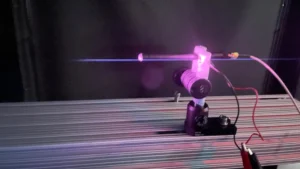
In a landmark development for the field of photonics, researchers at the California Institute of Technology (Caltech) have pioneered a method to transport light across silicon wafers with unprecedented efficiency, achieving signal loss levels at visible wavelengths that nearly mirror those of high-performance optical fibers. This breakthrough, detailed in the journal Nature, marks a significant shift in the design and manufacture of photonic integrated circuits (PICs). By successfully translating the ultra-low loss characteristics of long-haul optical fibers onto the compact architecture of a semiconductor chip, the team has paved the way for a new era of energy-efficient computing, high-precision sensing, and advanced quantum technologies.
The research, led by Kerry Vahala, the Ted and Ginger Jenkins Professor of Information Science and Technology and Applied Physics, addresses a long-standing bottleneck in the miniaturization of optical systems. While optical fibers have long served as the backbone of global communications due to their ability to carry light over vast distances with minimal degradation, replicating this performance on a silicon chip has historically proven elusive. The Caltech team’s success in bridging this gap suggests that the next generation of data centers, atomic clocks, and quantum computers could soon benefit from "fiber-like" performance in a footprint no larger than a postage stamp.
The Evolution of Optical Waveguides and the Silicon Challenge
To understand the magnitude of the Caltech achievement, one must first look at the history of optical communication. Since the 1970s, the purity of silica glass and the engineering of smooth internal surfaces have allowed optical fibers to transmit information across oceans with negligible loss. In these fibers, light is guided through a core with a higher refractive index than the surrounding cladding, a phenomenon known as total internal reflection.
However, when engineers attempted to replicate this on a chip—creating "waveguides" instead of fibers—they encountered significant hurdles. Traditional silicon-based manufacturing, while excellent for electronics, often results in waveguides with microscopic surface roughness. At the nanoscale, even atomic-level imperfections cause light to scatter, much like a car hitting a series of potholes. This scattering leads to "propagation loss," where the signal weakens rapidly as it travels.
For decades, the industry standard for low-loss PICs has been silicon nitride (Si3N4). While silicon nitride performs admirably in the near-infrared spectrum—the range typically used for telecommunications—its performance degrades significantly as it moves into the visible light spectrum (violet, blue, and green). The Caltech team recognized that to unlock the full potential of photonics, particularly for applications involving atomic systems and sensors, a new material and manufacturing philosophy were required.
Material Innovation: Bringing Germano-Silicate to the Wafer
The core of the Caltech breakthrough lies in the use of germano-silicate glass. This is the same material used in the core of high-quality optical fibers, prized for its transparency and refractive properties. The challenge, however, was not just using the material, but adapting it to the rigorous demands of lithography-based semiconductor manufacturing.
The research team, including lead authors Hao-Jing Chen and Kellan Colburn, developed a technique to print these optical circuits directly onto 8-inch and 12-inch silicon wafers—the standard sizes used in modern computer chip foundries. By integrating germano-silicate into a wafer-scale process, the researchers ensured that their discovery could be scaled for mass production, rather than remaining a laboratory curiosity.
One of the most innovative aspects of the design is the geometry of the waveguides. Rather than relying on straight paths, the researchers arranged the waveguides in intricate spirals. This design allows light to travel a much longer optical path—sometimes meters in length—while remaining confined within a tiny area on the chip. This "spool-on-a-chip" approach mimics the way optical fiber is wound for storage but does so with the precision of nanofabrication.
The "Reflow" Technique: Achieving Atomic Smoothness
The defining technical achievement that allowed the team to surpass existing benchmarks is a process known as "thermal reflow." Because germano-silicate has a lower melting temperature than traditional silicon-based materials, the researchers were able to heat the fabricated waveguides in a furnace.
During this heating phase, the surface of the glass becomes slightly molten. Surface tension then acts to smooth out any imperfections left behind by the etching and lithography processes. The result is a waveguide surface that is smooth down to the level of individual atoms.
"This largely suppresses the severe scattering loss that has limited conventional visible PICs," explained Hao-Jing Chen. The impact of this smoothness is most pronounced in the visible spectrum. According to the study, the germano-silicate platform exceeds the performance of silicon nitride—the previous record holder—by a factor of 20 at visible wavelengths. This 20-fold advantage is a transformative leap, as it allows for the creation of devices that were previously considered theoretically possible but practically unachievable due to energy dissipation.
Performance Metrics and Comparative Data
The data presented in the Nature paper highlights a dramatic improvement in coherence and energy efficiency. In the near-infrared range, the new platform matches the best-performing silicon nitride devices. However, as the wavelength decreases into the visible range, the germano-silicate waveguides maintain their ultra-low loss profile while other materials fail.
One of the most striking results involves the performance of lasers integrated with these waveguides. Laser coherence—the ability of a laser to maintain a consistent frequency over time—is critical for high-speed data transmission and precision measurements. The Caltech team found that lasers utilizing their new platform showed a 100-fold improvement in coherence over previous designs.
The mathematical relationship behind this is profound: the researchers noted that for every factor of 10 reduction in signal loss, the resulting laser coherence improves by a factor of 100. This exponential gain means that even incremental improvements in waveguide smoothness can lead to massive leaps in device performance.
Strategic Implications for AI and Data Centers
The practical applications of this technology are vast, with the most immediate impact likely to be felt in the realm of artificial intelligence and global data centers. Modern AI models require massive amounts of data to be moved between servers at lightning speeds. Currently, this data transfer relies heavily on electronic interconnects, which generate significant heat and consume vast amounts of electricity.
Henry Blauvelt, Chief Technology Officer at Emcore and a collaborator on the project, emphasized that the ability to efficiently transfer light between optical fibers and semiconductor lasers is "of paramount importance in reducing the overall energy cost of server infrastructure." By using ultra-low-loss waveguides, data centers can transition more of their internal communications to light-based systems, drastically reducing energy consumption and heat output. This could lead to more sustainable AI growth and more powerful supercomputing clusters.
Atomic Science and the Future of Quantum Computing
Beyond the data center, the Caltech breakthrough is set to revolutionize atomic and quantum science. Many of the most advanced technologies in development today, such as optical atomic clocks and ion-trap quantum computers, require the precise manipulation of atoms using visible light.
Until now, the high loss of visible light in integrated circuits meant that these systems often required bulky, table-top setups involving mirrors and lenses. The "fiber-like" performance of the new Caltech platform allows these complex optical setups to be shrunk down onto a single chip.
"The expanded wavelength coverage our method offers will support many important atomic operations, making chip-scale atomic sensors, optical clocks, and ion-trap systems possible," said Chen. This miniaturization is the key to moving quantum technology out of specialized laboratories and into real-world applications, such as ultra-precise GPS-free navigation and advanced medical imaging.
Chronology of Development and Collaborative Efforts
The success of this project is the culmination of over five years of intensive research within Kerry Vahala’s lab at Caltech. The journey began with the goal of translating the physics of long-distance fiber optics into the realm of integrated circuits.
- 2019-2021: Early experimentation with germano-silicate materials and the development of the "reflow" concept.
- 2022: Successful integration of the material onto standard 8-inch silicon wafers, proving scalability.
- 2023: Extensive testing across the spectrum, from violet (visible) to near-infrared, confirming the 20-fold advantage over silicon nitride.
- 2024: Publication of the findings in Nature and the demonstration of high-coherence lasers and ring resonators.
The project was a multi-institutional effort, reflecting the global interest in photonic integration. Contributors included researchers from UC Santa Barbara, Leiden University in the Netherlands, and the University of Southampton in the United Kingdom. The work was supported by several high-profile agencies, including the Defense Advanced Research Projects Agency (DARPA) and the Air Force Research Laboratory, highlighting the strategic and national security importance of high-performance photonics.
Conclusion: A New Standard for Photonic Integration
The development of ultra-low-loss germano-silicate waveguides represents a fundamental shift in how we think about light on a chip. By proving that the performance of a kilometer-long optical fiber can be condensed into a square centimeter of silicon, the Caltech team has removed one of the primary barriers to the "photonic revolution."
As Kerry Vahala noted, the technology has a "Swiss Army-knife quality," capable of being adapted for everything from the high-speed internet of the future to the quantum sensors of tomorrow. While the researchers acknowledge that they have not yet reached the absolute limit of what is possible, the current results set a new world record and provide a clear roadmap for further improvements.
As the industry looks toward 2030, the integration of visible-light photonics into standard semiconductor manufacturing will likely be viewed as a turning point. The ability to move light with "exceptionally little signal loss" is no longer just a characteristic of the cables buried under our streets; it is now a capability that resides in the very heart of the computer chip.