The pervasive challenge of thermal management, a phenomenon familiar to anyone whose laptop has grown uncomfortably warm during intensive tasks, represents one of the most significant hurdles in the advancement of global computing infrastructure. As computer chips become increasingly compact and powerful, the density of transistors packed into silicon wafers has reached a point where heat dissipation is no longer a secondary engineering concern but a primary bottleneck to performance. Addressing this crisis, a team of researchers at the Massachusetts Institute of Technology (MIT) has demonstrated a groundbreaking methodology for studying heat propagation through multilayered materials. By integrating high-intensity X-rays capable of penetrating multiple strata of a device with ultrafast laser pulses, the team has unlocked the ability to observe thermal dynamics at the micro- and nanoscale with unprecedented precision.
The research, recently published in the journal Nature Communications, arrives at a critical juncture for the semiconductor industry. As the world transitions toward more power-intensive applications—ranging from generative artificial intelligence and high-performance data centers to wearable health monitors and clean energy systems—the ability to manage "hotspots" within multilayered electronic architectures has become essential. Traditional measurement techniques have historically struggled to provide a clear picture of how heat moves through the complex, "club-sandwich" style stacks of materials that constitute modern transistors. The MIT-led innovation offers a "diagnostic window" into these buried layers, revealing how even microscopic defects can catastrophically impede the flow of heat.
The Invisible Bottleneck: Why Heat Management Matters
In the relentless pursuit of Moore’s Law—the observation that the number of transistors on a microchip doubles approximately every two years—engineers have successfully shrunk components to the nanometer scale. However, this miniaturization comes at a thermodynamic cost. When billions of transistors operate in close proximity, they generate immense amounts of thermal energy. If this heat is not efficiently moved away from the active components, the device suffers from "thermal throttling," where performance is intentionally capped to prevent physical damage, or worse, total hardware failure.
At the enterprise level, the implications are staggering. Global data centers, which power everything from cloud storage to AI training models, consume an estimated 1 percent of the world’s total electricity, a significant portion of which is dedicated solely to cooling systems. According to industry data, cooling can account for up to 40 percent of a data center’s total energy expenditure. For consumer electronics, overheating limits the battery life of wearables and the processing speed of smartphones.
"Chip developers need devices that can handle heat," explains Mingda Li, an associate professor of nuclear science and engineering at MIT and co-corresponding author of the study. "I think overheating has become the real bottleneck in device performance. When doing these diagnoses using traditional techniques, they couldn’t get down to the micro- or nanometer scale. But eventually, they’d like to go beyond that to study the heat carriers and understand exactly what causes failure, in order to avoid local hotspots and design better devices."
The Limitations of Legacy Measurement Tools
Before this breakthrough, the semiconductor industry relied on a handful of methods to model heat flow, each with significant drawbacks when applied to modern, multilayered architectures. One of the most common optical methods is Time Domain Thermal Reflectance (TDTR). While effective for surface-level analysis, TDTR relies on visible light, which cannot penetrate the various layers of a finished electronic device.
"Because that technique uses optics, it doesn’t allow you to study different layers," says Jeehwan Kim, an MIT associate professor and co-corresponding author. "Real devices have five or more layers. It also only provides an overall signal, and that makes it hard to see thermal transport happening in layers buried under the surface."
Other tools, such as infrared thermography, provide a broader thermal map but lack the spatial and temporal resolution required to see how heat moves at the atomic or molecular level. Infrared cameras operate at frame rates that are far too slow to capture the ultrafast transit of heat carriers across material interfaces. Consequently, engineers were often forced to rely on theoretical models that assumed "perfect" crystal structures—an assumption that rarely holds true in real-world manufacturing.
A Synergy of X-Rays and Lasers: How the New Technique Works
The MIT team’s approach overcomes these hurdles by utilizing an emerging analysis technique that pairs electron pulses and ultrafast X-rays with laser-induced heating. The experimentation was conducted in part at the Argonne National Laboratory, home to some of the brightest X-ray sources in the world.
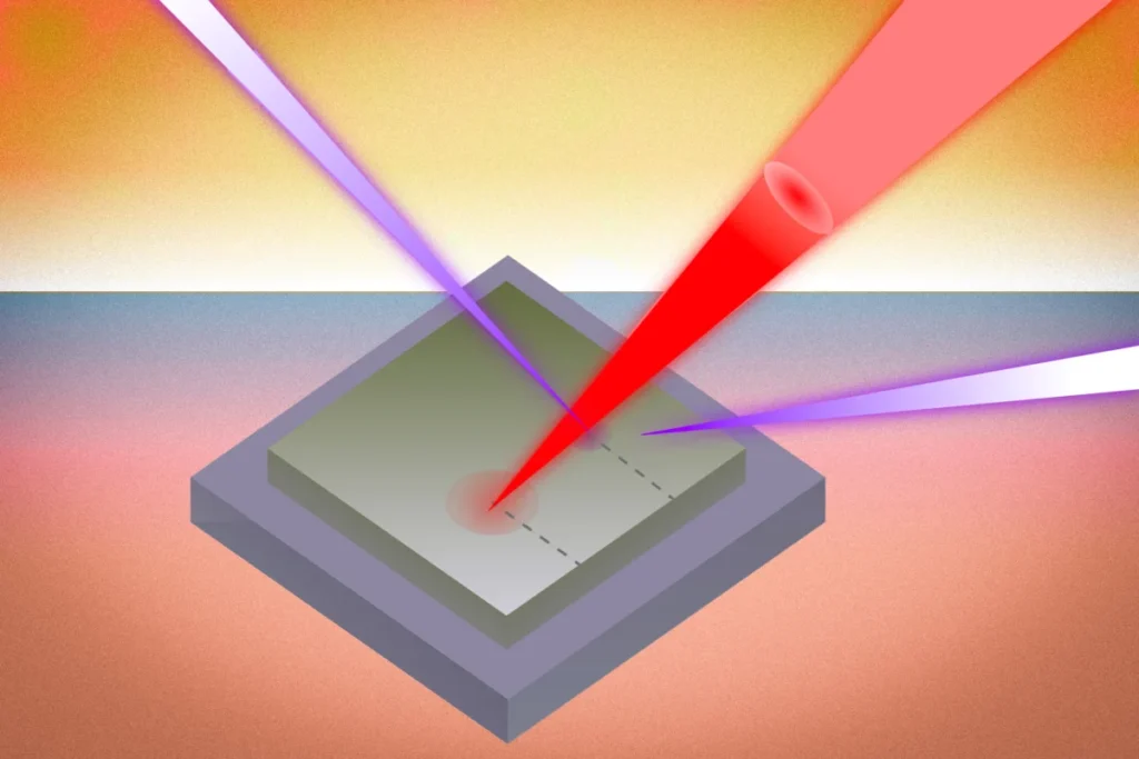
The process begins by using a laser to deliver a precise pulse of heat to a specific point on a sample material. Almost simultaneously, an ultrafast X-ray beam is directed at the device. Unlike visible light, X-rays possess the energy required to penetrate deep into the material stack. As the heat moves through the different layers, it causes the atomic lattice of the material to expand slightly—a phenomenon known as thermal strain.
By measuring the diffraction of the X-rays as they bounce off these atoms, the researchers can "see" the heat moving in real-time. This allows them to resolve what is happening on one specific layer versus another, rather than merely measuring an average temperature for the entire device.
"Over the last few years, researchers have developed what is basically the brightest X-ray source in the world," says co-lead author Thanh Nguyen. "That allows you to focus an X-ray beam and get incredibly fine spatial resolution. You can also use a laser to heat the sample while the X-ray scans and shows how the heat dissipates across space in real-time."
Case Study: The Hidden Impact of Micron-Scale Defects
To test the efficacy of their method, the researchers applied it to a promising material combination: gallium nitride (GaN) on a silicon substrate. Gallium nitride is widely considered a "miracle material" for the next generation of power electronics and 5G communications because of its high efficiency and ability to handle high voltages. However, during the manufacturing process, where thin films of GaN are grown on silicon, tiny physical defects such as wrinkles often occur.
Using their new X-ray technique, the MIT team quantified the impact of a single micron-scale wrinkle defect. The results were startling. They discovered a fourfold reduction in the material’s ability to transfer heat at the site of the defect. Furthermore, they found that the defect caused heat to spread unevenly—a phenomenon called anisotropy—where heat moved significantly easier in one direction than in the other.
"When people model heat dissipation, they model perfect crystals without defects," says Professor Li. "But these types of large wrinkle defects are very common in 2D materials. People never even knew how much heat is blocked by these wrinkles. Those are things we can now directly observe with this technique."
The discovery that a single, nearly invisible defect can slash thermal conductivity by 75 percent provides a definitive explanation for why many high-performance chips fail prematurely or underperform in the field.
Chronology of Development and Collaborative Effort
The development of this technique is the result of years of interdisciplinary collaboration involving experts in nuclear science, mechanical engineering, materials science, and physics.
- 2018–2021: Initial conceptualization of using X-ray diffraction to monitor thermal strain in semiconductor heterostructures.
- 2022–2023: Refinement of the ultrafast laser-X-ray synchronization at national laboratory facilities, allowing for picosecond-scale temporal resolution.
- 2024: Successful application of the technique to Gallium Nitride-on-Silicon devices and the quantification of wrinkle-defect thermal resistance.
- Present: Engagement with a leading semiconductor industry consortium to integrate this diagnostic tool into commercial R&D pipelines.
The research team included a diverse group of scholars from MIT, the University of Texas at Austin, and Argonne National Laboratory. The work received financial backing from the U.S. Department of Energy (DOE), the U.S. National Science Foundation (NSF), and the MIT School of Engineering.
Industry Implications: AI, Clean Energy, and Beyond
The semiconductor industry is already taking note. As companies like NVIDIA, Intel, and TSMC race to produce chips for the AI revolution, the "thermal wall" has become their primary adversary. AI chips, which require massive amounts of power to process trillions of operations per second, generate heat at densities that threaten to melt the very circuits they reside on.
"We can now pass a current and shine an X-ray on a device and see how the heat dissipates at a very small scale," says Professor Kim. "That’s something the industry has been longing for."
Beyond computing, the technique has profound implications for:
- Electric Vehicles (EVs): Power inverters in EVs rely on GaN and Silicon Carbide (SiC) chips. Improving the thermal design of these components can lead to faster charging times and longer range.
- Flexible Electronics: For wearable devices that sit directly on human skin, managing heat is a safety requirement. This technique allows for the design of flexible circuits that stay cool.
- Clean Energy Systems: Solar inverters and grid-scale storage systems require durable electronics that can withstand high thermal stress over decades.
A New Paradigm for Electronic Design
The MIT researchers believe their approach will fundamentally change how electronic systems are designed. Instead of over-engineering cooling systems (like massive fans or liquid cooling) to compensate for unknown thermal bottlenecks, engineers can now use "thermal-aware design." By identifying exactly where heat gets trapped—whether at a material interface or a manufacturing defect—they can rearrange the geometry of the chip to facilitate natural flow.
"Even with the same type of materials, the geometry and how the materials are laid out is quite complicated," Kim notes. "This will show us how those differences impact thermal flow by providing direct experimental measurements."
As the semiconductor industry moves toward 3D-stacked chips (where multiple layers of logic and memory are piled on top of each other), the "X-ray vision" provided by this MIT research will likely become an indispensable tool in the quest to keep the digital world running cool. By moving from theoretical models to direct observation, the industry is now one step closer to overcoming the thermal bottleneck and unlocking the next generation of technological innovation.