Quantum computers today are notoriously difficult and expensive to operate, demanding environments near absolute zero, approximately -459 degrees Fahrenheit (-273.15 degrees Celsius or 0 Kelvin), to maintain the exquisitely fragile quantum states essential for computation and communication. This cryogenic necessity has been a significant barrier to the widespread adoption and miniaturization of quantum systems, confining most advanced research to specialized laboratories equipped with colossal dilution refrigerators. However, a recent development from Stanford University promises to dismantle this formidable obstacle, with researchers unveiling a nanoscale optical device that achieves stable quantum entanglement between light and electrons at ambient room temperatures. This groundbreaking advance, detailed in a study published in Nature Communications, could fundamentally alter the trajectory of quantum technology, ushering in an era of smaller, lower-cost, and more deployable quantum devices capable of transmitting information across vast distances without the need for extreme cooling infrastructure.
The core of this innovation lies in the device’s ability to create entanglement between photons—the fundamental particles of light—and electrons, a quantum connection considered a foundational requirement for the architecture of future quantum communication networks. This photon-electron entanglement is crucial because photons are ideal carriers for long-distance quantum information, while electrons, particularly their spin states, are excellent for storing and processing quantum data. Bridging these two realms efficiently and stably at room temperature represents a monumental leap forward, addressing one of the most persistent challenges in quantum science: decoherence, the rapid loss of delicate quantum information due to environmental interference.
"The material in question is not really new, but the way we use it is," explains Jennifer Dionne, a professor of materials science and engineering at Stanford and senior author of the study. Her statement underscores the ingenuity of the approach, which leverages known materials in a novel configuration. "It provides a very versatile, stable spin connection between electrons and photons that is the theoretical basis of quantum communication. Typically, however, the electrons lose their spin too quickly to be useful." This quick loss of electron spin, a form of quantum information, is precisely what the Stanford team has managed to mitigate, offering a robust platform for maintaining quantum coherence.
The Cryogenic Conundrum: A Historical Context for Quantum Computing
For decades, the pursuit of quantum computing has been intrinsically linked to the quest for ultracold temperatures. The reason is rooted in the very nature of quantum mechanics. Quantum bits, or qubits, unlike classical bits that are either 0 or 1, can exist in a superposition of both states simultaneously. They can also be entangled, meaning their fates are intertwined regardless of distance. These phenomena are incredibly delicate and susceptible to disruption by thermal energy. At room temperature, atoms and electrons are constantly vibrating and interacting, causing qubits to quickly lose their quantum properties through a process called decoherence.
To counteract this, many leading quantum computing architectures—such as those based on superconducting circuits—are housed within dilution refrigerators that cool them to temperatures mere thousandths of a degree above absolute zero (millikelvin range). These cryostats are massive, expensive, and consume significant power, often costing millions of dollars and requiring specialized infrastructure. For instance, a typical 64-qubit superconducting quantum computer can occupy a volume equivalent to a small car, with the cryogenic system being the largest component. This immense infrastructure limits quantum computers to highly specialized research facilities, making them impractical for widespread deployment or integration into existing technological frameworks. The historical trajectory of quantum research has therefore been a constant battle against thermal noise, with each incremental improvement in coherence time often necessitating even lower temperatures or more isolated environments. The ability to sidestep these extreme cooling requirements has long been considered a "holy grail" in the field, promising to unlock new avenues for practical quantum technologies.
Twisted Light and Quantum Spin: The Mechanism of Entanglement
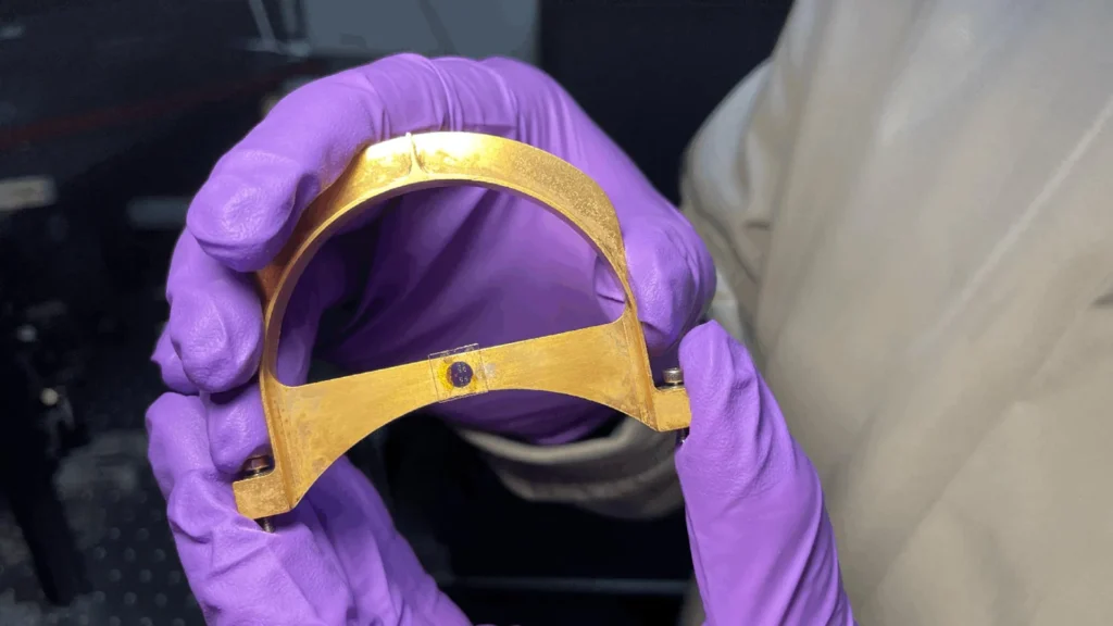
The Stanford device’s innovation lies in its unique architecture, combining a thin, patterned layer of molybdenum diselenide (MoSe2) with a nanopatterned silicon substrate. Molybdenum diselenide belongs to a fascinating class of materials known as transition metal dichalcogenides (TMDCs). These two-dimensional materials, similar to graphene but with semiconducting properties, are highly valued for their exceptional optical and quantum characteristics, including strong light-matter interaction and distinct spin-valley coupling, which makes them ideal candidates for optoelectronic and spintronic applications.
The true genius of the Stanford design, however, lies in the role played by the silicon nanostructures. These meticulously engineered structures are critical for generating what the researchers term "twisted light." Feng Pan, a postdoctoral scholar in Dionne’s lab and the paper’s first author, elaborates on this phenomenon: "The silicon nanostructures enable what we call ‘twisted light.’ The photons spin in a corkscrew fashion, but more importantly, we can use these spinning photons to impart spin on electrons that are the heart of quantum computing." This "twisted light" is essentially circularly polarized light with an added orbital angular momentum, which allows for a more efficient and precise transfer of angular momentum (and thus spin) to the electrons within the MoSe2 layer.
Dionne emphasizes the microscopic scale of these patterned structures, noting their dimensions are "incredibly small, roughly comparable in size to visible light wavelengths and impossible to see with the naked eye." She adds, "The patterned nanostructures are imperceptible to the human eye, about the size of the wavelength of visible light. But they help us manipulate photons very precisely to make them spin—to twist them—in a specific direction, for example, up or down." This precise manipulation of photons at the nanoscale is what enables the stable, room-temperature entanglement. By carefully controlling the orbital angular momentum of the photons, the researchers can effectively ‘tune’ the spin state of the electrons in the MoSe2, establishing a robust quantum link between light and matter.
A Simpler Path to Quantum Communication and Computing
The ability to use this twisted light to entangle with electron spins is fundamental to creating qubits, the basic building blocks of quantum information systems. In conventional computing, information is represented by binary bits, either 0 or 1. Quantum technologies, however, leverage the unique principles of quantum mechanics—superposition and entanglement—to allow qubits to represent multiple states simultaneously, enabling entirely new paradigms for processing and transmitting information.
One of the most formidable challenges facing quantum technologies, as previously noted, is maintaining stable quantum states for long enough to perform useful computations or communication. This susceptibility to environmental noise, leading to decoherence, is why extreme cooling has historically been indispensable. The Stanford device’s breakthrough in operating at room temperature directly tackles this major hurdle, circumventing the need for the elaborate and costly cryogenic infrastructure that has limited the widespread deployment of quantum technologies.
The implications of this room-temperature functionality are profound. Firstly, it drastically reduces the overall cost and complexity of quantum systems. The elimination of million-dollar cryostats, along with their associated operational expenses and maintenance, makes quantum devices significantly more accessible. Secondly, the compact, chip-scale design of the new device is inherently more practical for integration into existing technological frameworks. Imagine quantum components that can be incorporated into standard data centers, telecommunication networks, or even portable devices, rather than being confined to bespoke, refrigerator-sized installations. This miniaturization and cost reduction could accelerate the transition of quantum research from the lab to real-world applications.
Broader Impact and Future Implications
If further developed and scaled, this technology could contribute to transformative advances across a spectrum of fields. In secure communications, it could underpin the development of truly unhackable quantum communication networks, such as a quantum internet. By leveraging the principles of quantum key distribution (QKD), where any attempt to eavesdrop on a communication channel instantly alters the quantum state and is thus detected, this technology could enable unprecedented levels of data security for governments, financial institutions, and critical infrastructure. Current QKD systems often face limitations in distance and require complex setups; a room-temperature, chip-scale entangling device could simplify and extend their reach.
In advanced sensing, quantum effects can lead to sensors with unparalleled precision, capable of detecting minute changes in magnetic fields, gravity, or temperature. Room-temperature quantum sensors could be deployed in medical diagnostics, geological surveys, or navigation systems with greater flexibility and lower operational overhead. For high-performance computing and artificial intelligence, while direct quantum computation in a cell phone is still a distant goal, these room-temperature entanglement sources could serve as crucial interfaces for hybrid quantum-classical computing architectures, or as components in distributed quantum networks that collectively tackle complex problems. The ability to link quantum nodes without cryogenic cooling could enable more robust and scalable quantum network designs, paving the way for a truly interconnected quantum internet.
Why the Material Matters: The Synergy of MoSe2 and Silicon
The choice of materials was pivotal to the Stanford team’s success. As Pan explains, "It all comes down to this material and our silicon chip. Together, they efficiently confine and enhance the twisting of light to create a strong coupling of spin between photons and electrons. This stabilizes the quantum state that makes quantum communication possible." The team specifically selected TMDC materials like molybdenum diselenide due to their unusual quantum characteristics. They collaborated with Stanford researchers Fang Liu and Tony Heinz, experts in these materials, to optimize the material’s properties for the device.
Monolayer TMDCs possess a direct bandgap, meaning they efficiently absorb and emit light, making them excellent candidates for optoelectronic applications. More importantly, their electronic structure exhibits strong spin-orbit coupling and valley degrees of freedom, which means the spin of an electron is intimately linked to its momentum state (its "valley"). This inherent property facilitates the transfer of spin information from circularly polarized light (or "twisted light") to the electrons, and vice versa. The silicon nanostructures, in turn, are engineered to precisely sculpt the light, converting incident light into the desired "twisted light" with controlled orbital angular momentum. This synergistic combination allows for an enhanced light-matter interaction, providing a stable and efficient mechanism for preserving the delicate quantum properties necessary for communication and computing tasks, even at room temperature. The precision of the nanoscale patterning on the silicon is crucial, enabling the researchers to effectively control the light’s properties at a scale comparable to its wavelength.
Toward Future Quantum Networks and Everyday Integration
The Stanford researchers are not resting on their laurels. They are actively pursuing improvements to the device, exploring additional TMDC materials and material combinations that could yield even better performance, potentially offering longer coherence times or higher entanglement fidelities. They are also investigating whether these room-temperature systems might unveil entirely new quantum capabilities that are currently unattainable in cryogenically cooled environments, perhaps due to different interaction dynamics at higher temperatures.
A longer-term, yet highly ambitious, goal is the integration of devices like this into larger, distributed quantum networks. Achieving this vision will necessitate parallel advancements in supporting technologies, including more efficient light sources, high-speed modulators for encoding information onto photons, highly sensitive detectors, and robust interconnects to link multiple quantum nodes. The development of a scalable quantum internet, capable of transmitting entangled qubits across continents, hinges on such foundational breakthroughs.
Ultimately, the aspiration is for quantum components to be miniaturized sufficiently to be incorporated into everyday electronics. While that future remains many years away—a "10-plus-year plan," as Pan lightheartedly suggests—the work by the Stanford team represents a monumental step toward making quantum technology more accessible, practical, and ubiquitous. By decoupling quantum functionality from the restrictive demands of cryogenic cooling, this research significantly broadens the potential applications of quantum science, moving it from the realm of esoteric laboratory experiments into the tangible possibility of impacting daily life, one quantum chip at a time. The implications for national security, economic competitiveness, and scientific discovery are profound, marking a pivotal moment in the ongoing quantum revolution.