Quantum computers, long hailed as the next frontier in computational power, currently face formidable operational challenges, primarily stemming from their extreme environmental requirements. Most existing quantum systems demand temperatures hovering near absolute zero, a chilling -459 degrees Fahrenheit, to sustain the incredibly fragile quantum states essential for computation and communication. This necessity translates into colossal infrastructure, exorbitant costs, and significant operational complexities, severely limiting their scalability and widespread adoption. However, a recent breakthrough from Stanford University promises to redefine this landscape, with researchers developing a nanoscale optical device capable of operating at room temperature while effectively linking the quantum properties of light and electrons. This advancement could be a pivotal step towards developing smaller, more affordable quantum technologies, particularly those designed for transmitting information across vast distances.
Overcoming the Quantum Chill: A New Paradigm
The innovative device marks a significant stride in quantum engineering, primarily by addressing the persistent challenge of environmental sensitivity. By enabling entanglement between photons—the fundamental particles of light—and electrons at ambient temperatures, the Stanford team has tackled a core hurdle in the development of practical quantum communication systems. Entanglement, a bizarre quantum phenomenon where two particles become inextricably linked, sharing the same fate regardless of distance, is considered an indispensable prerequisite for future quantum networks.
"The material in question is not really new, but the way we use it is," explains Jennifer Dionne, a professor of materials science and engineering at Stanford and the senior author of the study, which was published in the prestigious journal Nature Communications. Dionne elaborates on the device’s fundamental utility: "It provides a very versatile, stable spin connection between electrons and photons that is the theoretical basis of quantum communication. Typically, however, the electrons lose their spin too quickly to be useful, making this stability at room temperature particularly noteworthy." This stability, achieved without the need for cryogenic cooling, represents a monumental leap forward, circumventing the primary barrier of decoherence—the loss of quantum information due to interaction with the environment—that has plagued quantum systems for decades.
The Architecture of Innovation: Twisted Light and Quantum Spin
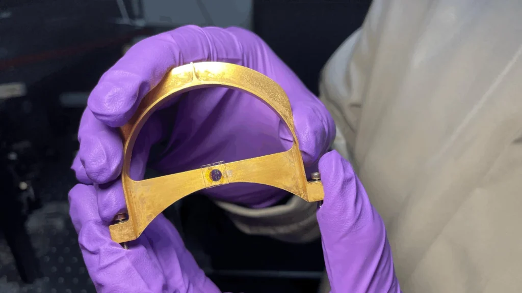
At the heart of this groundbreaking device lies a sophisticated combination of advanced materials and nanophotonics. It integrates a thin, intricately patterned layer of molybdenum diselenide (MoSe2) with a nanopatterned silicon substrate. Molybdenum diselenide belongs to a class of materials known as transition metal dichalcogenides (TMDCs), which have garnered considerable scientific interest due to their exceptional optical and quantum properties. These materials exhibit strong light-matter interaction and possess unique electronic band structures that make them ideal candidates for quantum applications.
Crucially, the silicon nanostructures embedded within the device play a transformative role by generating what the researchers term "twisted light." Feng Pan, a postdoctoral scholar in Dionne’s lab and the paper’s first author, elucidates this mechanism: "The silicon nanostructures enable what we call ‘twisted light.’ The photons spin in a corkscrew fashion, but more importantly, we can use these spinning photons to impart spin on electrons that are the heart of quantum computing." This "twisted light" refers to photons carrying orbital angular momentum (OAM), a property that can be precisely controlled and transferred.
Dionne emphasizes the minute scale of these critical components. "The patterned nanostructures are imperceptible to the human eye, about the size of the wavelength of visible light," she notes. "But they help us manipulate photons very precisely to make them spin—to twist them—in a specific direction, for example, up or down." This exquisite control over photon properties at the nanoscale is what allows for the efficient and stable transfer of quantum information between light and matter. The ability to impart spin from twisted photons to electrons creates a robust, entangled state that is far more resilient to environmental interference than previously achieved at room temperature.
A Simpler Path to Quantum Communication and Beyond
The creation of entanglement between twisted light and electron spins forms the basic building blocks of quantum information systems, known as qubits. Unlike conventional computing, where information is represented by binary zeros and ones, qubits leverage quantum mechanical effects such as superposition (being in multiple states simultaneously) and entanglement to process and transmit information in entirely novel ways. The stability of these qubits is paramount, and the new Stanford device offers an unprecedented pathway to maintaining them.
One of the most formidable challenges facing the entire quantum technology landscape has been maintaining stable quantum states. In the majority of existing quantum computing and communication systems, extreme cooling—often to millikelvin temperatures, just fractions of a degree above absolute zero—is indispensable. This super-cooling is necessary to minimize thermal noise and prevent decoherence, a process where delicate quantum information is rapidly lost due to interaction with the surrounding environment. The engineering feat of achieving and maintaining these ultra-low temperatures involves complex and expensive cryogenic systems, vacuum chambers, and elaborate vibration isolation, significantly inflating the cost and physical footprint of quantum devices.
By operating at room temperature, the Stanford device sidesteps one of the most prohibitive obstacles that has historically limited the widespread utility and commercialization of quantum technologies. The researchers also highlight the compact and relatively inexpensive design of their device, presenting it as a practical alternative to many current quantum systems. This reduction in complexity and cost is not merely an engineering convenience; it represents a fundamental shift in the feasibility of deploying quantum technologies outside specialized, highly controlled laboratory environments.
If further developed and scaled, this technology could unlock transformative advancements across numerous sectors. Potential applications include ultra-secure communications through quantum key distribution (QKD), distributed quantum computing where multiple quantum processors work in concert, advanced sensing capabilities far beyond classical limits, and accelerating developments in high-performance computing and artificial intelligence. The implications for industries ranging from finance and healthcare to defense and aerospace are profound, promising capabilities previously confined to the realm of science fiction.
The Crucial Role of Material Science
The selection of TMDC materials was a deliberate choice, driven by their unique quantum characteristics. The Stanford team collaborated with specialists in these materials, Fang Liu and Tony Heinz, to leverage their expertise. "It all comes down to this material and our silicon chip," Pan reiterates. "Together, they efficiently confine and enhance the twisting of light to create a strong coupling of spin between photons and electrons. This stabilizes the quantum state that makes quantum communication possible."
TMDCs, such as molybdenum diselenide, are two-dimensional materials with properties that bridge the gap between semiconductors and insulators. Their atomic thinness (often just a few layers thick) allows for strong exciton binding energies, meaning that electron-hole pairs (excitons) within the material are very stable and interact strongly with light. This strong light-matter interaction, coupled with their unique spin-valley physics (where electron spin is coupled to specific energy minima in their electronic band structure), makes them exceptional platforms for quantum information processing. The combined architecture effectively harnesses these intrinsic properties, allowing for the stable and efficient preservation of quantum properties necessary for demanding communication and computing tasks.
Toward Future Quantum Networks: A Long-Term Vision
The Stanford researchers are not resting on their laurels; their work is an ongoing endeavor. They are actively engaged in improving the device’s performance, exploring other TMDC materials, and investigating novel material combinations that could yield even greater efficiencies and functionalities. A particularly exciting avenue of research involves probing whether these room-temperature systems might reveal entirely new quantum capabilities that are currently inaccessible or unobservable under conventional cryogenic conditions.
A more ambitious, longer-term objective is the integration of these compact, room-temperature devices into larger, distributed quantum networks. Achieving this vision will necessitate parallel advancements in a host of supporting technologies, including more efficient and tunable light sources, high-speed modulators, ultra-sensitive detectors, and robust quantum interconnects capable of linking disparate quantum nodes. The development of a "quantum internet" that can securely transmit quantum information globally relies heavily on such practical, scalable components.
Ultimately, the aspiration is to miniaturize quantum components to a degree where they can be seamlessly incorporated into everyday electronics, making quantum technology pervasive and accessible. While acknowledging that such a future remains many years, if not decades, away, the work at Stanford represents a concrete and significant step toward making quantum technology more practical, affordable, and broadly applicable.
"If we can do that, maybe someday we could do quantum computing in a cell phone," Pan muses with a smile, outlining a vision that, while ambitious, is now slightly less distant. "But that’s a 10-plus-year plan." This perspective underscores both the monumental progress achieved and the vast intellectual and engineering challenges that still lie ahead on the path to a fully quantum-enabled world. This Stanford breakthrough provides a critical building block, moving quantum technology from the frigid confines of specialized labs closer to the warmth of everyday utility.