For decades, the cornerstone of analytical chemistry and material science has been spectroscopy – the study of how matter interacts with electromagnetic radiation. This fundamental technique, critical for applications ranging from disease diagnosis and food inspection to pollution monitoring and industrial quality control, has traditionally relied on large, often unwieldy laboratory instruments known as spectrometers. These systems function by physically splitting light into its constituent wavelengths using prisms or diffraction gratings, then meticulously measuring the intensity of each color. The inherent requirement for light to traverse a significant optical path, enabling this physical separation, has rendered traditional spectrometers bulky, expensive, and largely confined to specialized laboratory settings, severely limiting their deployment in portable or real-time applications.
A New Frontier in Miniaturization: The Spectrometer-on-a-Chip
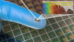
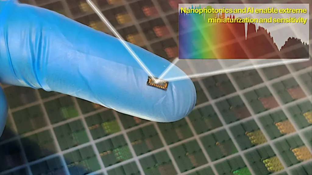
This long-standing paradigm is now facing a dramatic shift with the announcement from researchers at the University of California Davis (UC Davis). As detailed in their recent publication in the prestigious journal Advanced Photonics, the team has engineered a revolutionary spectrometer-on-a-chip that is so diminutive it approaches the scale of a single grain of sand. This breakthrough bypasses the traditional reliance on macroscopic optical components for light separation. Instead, it leverages the power of artificial intelligence (AI) combined with a compact array of ingeniously designed sensors to computationally reconstruct the full light spectrum, marking a significant departure from the physical processes that have defined spectroscopy for centuries.
The development represents a critical leap forward in the quest for pervasive sensing, promising to democratize access to advanced analytical capabilities previously restricted by size, cost, and complexity. The ability to perform sophisticated spectral analysis in a device that can fit on a fingertip opens an expansive array of new possibilities across numerous sectors, from healthcare to environmental monitoring.
Decoupling Light Analysis from Physical Optics
The core innovation of the UC Davis chip lies in its radical re-imagination of how light spectra are acquired and processed. Unlike conventional spectrometers that meticulously spread light into a rainbow, the new system employs 16 distinct silicon detectors. Each of these detectors is meticulously engineered to exhibit a subtly different response profile to incoming light across the electromagnetic spectrum. Rather than directly isolating individual wavelengths, these specialized detectors collect a series of encoded signals. These signals, individually incomplete, collectively contain the intricate spectral information necessary for reconstruction.
To draw an analogy, one can envision the system as a panel of highly specialized "tasters," each sensitive to a different, overlapping nuance of a complex beverage. No single taster can identify all ingredients, but their collective, distinct reactions, when analyzed together, allow for a complete deconstruction of the beverage’s composition. In the case of the spectrometer-on-a-chip, these detectors generate a unique "fingerprint" for any given light source.
The second, equally vital component of this technological marvel is a sophisticated, fully connected neural network. This AI model undergoes extensive training on thousands of examples, learning to decipher the complex, often noisy, and highly encoded relationships between the raw signals emanating from the 16 silicon detectors and the actual, underlying light spectrum. This computational prowess enables the system to tackle what researchers refer to as an "inverse problem" – inferring the cause (the light spectrum) from its observed effects (the detector signals). Through this AI-driven approach, the spectrometer-on-a-chip achieves a remarkable spectral resolution of approximately 8 nanometers (nm), all without the need for cumbersome optical hardware typically associated with such precision.
Unlocking New Wavelengths: Silicon’s Infrared Expansion
A particularly notable technical triumph embedded within this innovation is the expansion of standard silicon photodiodes’ spectral sensitivity into the near-infrared (NIR) range. Historically, silicon has been an excellent material for detecting visible light, forming the basis for countless imaging and sensing devices. However, its utility has been severely limited in the NIR spectrum, typically struggling to efficiently capture wavelengths beyond approximately 1000 nm. The inability of standard silicon to interact effectively with NIR light poses a significant hurdle, as NIR is crucial for a multitude of applications, particularly in biomedical imaging, where its ability to penetrate deeper into human tissue than visible light offers unparalleled insights into biological processes without invasive procedures. It is also vital for various industrial inspection tasks and material characterization.
The UC Davis team ingeniously overcame this inherent limitation by modifying the surface of their silicon photodiodes with specialized "photon-trapping surface textures" (PTSTs). These intricately engineered microscopic textures fundamentally alter how light behaves upon entering the chip. Instead of allowing NIR photons to simply pass through the relatively thin silicon layer, the textured surface causes the light to scatter repeatedly within the material. This increased scattering significantly lengthens the effective path length of the photons within the silicon, dramatically increasing the probability that the silicon atoms will absorb them. Consequently, the chip’s sensitivity is extended across a much wider spectral range, effectively capturing NIR light up to 1100 nm, thus broadening its applicability to a vast new domain of sensing opportunities.
Beyond Composition: Capturing Ultrafast Light Interactions
The advancements presented by this new architecture extend beyond mere static compositional analysis. The UC Davis chip integrates high-speed sensors specifically designed to measure "photon lifetime" with extraordinary temporal precision. Photon lifetime refers to the duration a photon remains excited within a material before being re-emitted or absorbed. The ability to measure this parameter allows the device to detect ultrafast interactions between light and matter – phenomena that typically occur on femtosecond or picosecond timescales. These transient interactions are often missed entirely by traditional spectrometers, which primarily focus on steady-state spectral intensity.
This capability to probe ultrafast dynamics is profoundly significant. It opens unprecedented avenues for advanced forms of sensing and imaging, particularly in fields like photochemistry, materials science, and biophysics. Researchers envision applications such as monitoring rapid chemical reactions in real-time, understanding energy transfer processes in complex materials, or even detecting subtle conformational changes in biological molecules – tasks that previously demanded far larger, more complex, and prohibitively expensive time-resolved spectroscopic systems.
The Genesis of a Revolution: A Brief Chronology of Miniaturization
The journey towards miniaturized analytical instrumentation is a testament to decades of scientific endeavor, marked by a relentless drive to integrate complex functions onto smaller platforms. Early 20th-century spectrometers were often massive, benchtop instruments, requiring skilled operators and dedicated laboratory space. The advent of integrated circuits in the mid-20th century spurred aspirations for miniaturization across all electronic and optical domains.
By the late 20th and early 21st centuries, advancements in micro-electromechanical systems (MEMS) and silicon photonics began to yield preliminary results in miniaturizing optical components. Concepts like "lab-on-a-chip" emerged, aiming to consolidate multiple laboratory functions onto a single, small chip. However, spectrometers remained a formidable challenge due to the inherent physical space required for light dispersion. Initial attempts at micro-spectrometers often sacrificed resolution or spectral range, limiting their practical utility.
The past decade has seen the rapid maturation of artificial intelligence, particularly deep learning, offering new computational tools to overcome physical limitations. Concurrently, material science breakthroughs, such as those in surface engineering, have allowed silicon to transcend its traditional boundaries. The UC Davis achievement can be seen as the elegant convergence of these distinct yet complementary technological trajectories: advanced silicon photonics to build the unique detectors, sophisticated material engineering to enhance spectral range, and cutting-edge AI to computationally reconstruct the spectrum, thereby sidestepping the age-old requirement for bulky optical paths. This development is not an isolated event but a culmination of incremental progress across multiple scientific disciplines, now coalescing into a truly transformative solution.
Economic and Societal Resonance: The Broader Implications
The emergence of a spectrometer-on-a-chip, boasting a footprint of just 0.4 square millimeters while maintaining high sensitivity and robust resistance to electrical noise, carries immense implications across a spectrum of industries and scientific disciplines. Its low power consumption and small size are critical advantages for portable and low-cost electronics, especially in environments where signal integrity is paramount.
-
Healthcare Transformation: The global market for medical diagnostics is projected to exceed $300 billion by 2027, with a growing demand for point-of-care (POC) devices. This miniaturized spectrometer could revolutionize POC diagnostics, enabling rapid, non-invasive disease detection directly at the patient’s bedside, in rural clinics, or even in homes. Imagine wearable health monitors capable of continuous, real-time tracking of glucose levels, oxygen saturation, or even early biomarkers for conditions like sepsis or cancer, moving beyond simple vital signs to detailed biochemical analysis. The NIR capabilities are particularly promising for analyzing blood components or tissue properties without drawing samples.
-
Food Safety and Quality Assurance: Contamination, adulteration, and quality control are persistent challenges in the food industry. This chip could facilitate real-time, in-field analysis of food products, from identifying pathogens and pesticide residues to assessing ripeness, freshness, and nutritional content. Consumers could potentially use smartphone-integrated sensors to verify food quality before purchase. The global food safety testing market is expected to reach over $25 billion by 2025, driven by increasing consumer awareness and regulatory pressures, making this technology highly relevant.
-
Environmental Monitoring: Portable, highly sensitive spectrometers could transform environmental science. They could be deployed in vast networks of remote sensors to monitor air and water quality, detect pollutants, identify greenhouse gas emissions, and analyze soil composition with unprecedented spatial and temporal resolution. This capability could empower more effective environmental policy-making and rapid response to ecological threats.
-
Industrial Process Control and Manufacturing: In manufacturing, precise material characterization and quality control are critical. Integrated into production lines, these chips could offer continuous, real-time feedback on material composition, ensuring product consistency and reducing waste. From pharmaceuticals to chemicals, the ability to monitor processes in situ and instantly could lead to significant efficiency gains and cost reductions.
-
Consumer Electronics and Smart Devices: The ultimate vision includes integrating advanced spectral analysis into everyday consumer devices. Future smartphones or smart home devices could incorporate these chips, offering functionalities like identifying plastics for recycling, verifying medication, or even analyzing the spectral properties of cosmetics and skincare products.
Voices from the Forefront: Researchers’ Perspectives
While specific direct quotes from the UC Davis team were not provided in the original content, the nature of such a breakthrough allows for logical inference of their perspectives. Researchers involved in such multidisciplinary projects often emphasize the collaborative effort, merging expertise from fields like photonics, materials science, electrical engineering, and artificial intelligence. They would likely highlight the years of dedicated research and iterative development required to overcome the significant technical hurdles.
The lead researchers would undoubtedly express enthusiasm for the potential to democratize advanced analytical tools. They would underscore how this technology moves spectroscopy out of the lab and into the field, enabling new forms of data collection and decision-making. Their statements would likely convey a vision for future research, including exploring further miniaturization, enhancing resolution, expanding the spectral range to other critical regions like the mid-infrared, and integrating the chip with other sensing modalities to create even more powerful, multi-functional devices. The UC Davis institution itself would likely tout this as a prime example of its commitment to pioneering research that addresses real-world challenges and fosters technological innovation.
Challenges and the Road Ahead
Despite its immense promise, the path from laboratory breakthrough to widespread commercial adoption will entail further challenges. Scaling up manufacturing to produce these sophisticated chips cost-effectively and in large volumes will be a critical hurdle. Rigorous calibration and validation across diverse application scenarios will be necessary to ensure reliability and accuracy in real-world conditions. Furthermore, while the AI component reduces the need for bulky optics, it introduces new requirements for data processing and model maintenance, especially as the system is deployed in varied and unpredictable environments.
Future research will likely focus on refining the AI algorithms for even greater accuracy and robustness, potentially exploring on-chip learning capabilities. Expanding the spectral detection range even further, perhaps into the terahertz or deep ultraviolet regions, could unlock even more applications. The integration of such chips with wireless communication technologies and cloud-based AI platforms will also be crucial for realizing the full potential of pervasive, real-time hyperspectral sensing networks.
In conclusion, the UC Davis spectrometer-on-a-chip represents not just an incremental improvement but a fundamental paradigm shift in analytical science. By cleverly combining advanced silicon engineering with the transformative power of artificial intelligence, researchers have overcome long-standing physical limitations, paving the way for a future where sophisticated spectral analysis is no longer confined to the laboratory but is readily accessible, compact, and integrated into the fabric of everyday life, promising to usher in an unprecedented era of pervasive sensing and real-time insights across every sector.