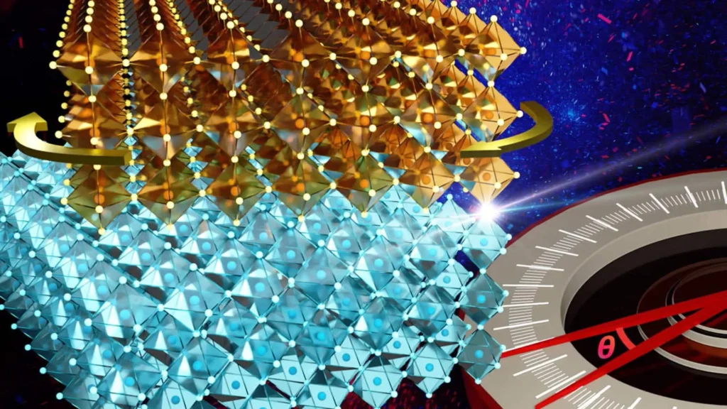
Researchers at North Carolina State University have announced a significant leap forward in the field of condensed matter physics, developing a methodology that allows for the creation of twisted oxide materials over significantly larger surface areas than previously possible. By maintaining nanometer-scale precision over the rotational alignment of layered crystalline membranes, the team has successfully bridged the gap between theoretical "twistronics" and practical, scalable electronic applications. This development, published in the journal ACS Nano, addresses one of the most persistent bottlenecks in the development of next-generation electronics: the difficulty of manipulating materials with strong chemical bonds at a macroscopic scale.
The field of twistronics, a term coined to describe the study of how the relative rotation between layers of two-dimensional materials can radically alter their physical and electronic properties, has predominantly been confined to the realm of van der Waals materials. These are substances, such as graphene or hexagonal boron nitride, where layers are held together by relatively weak intermolecular forces. However, the NC State team, led by Assistant Professor Ruijuan Xu, has demonstrated that these same principles can be applied to complex oxides—materials characterized by much stronger chemical bonds and a diverse array of functional properties, including superconductivity, ferroelectricity, and magnetism.
The Evolution of Twistronics: From Graphene to Complex Oxides
To understand the magnitude of this advancement, one must look at the trajectory of material science over the last decade. In 2018, the scientific community was electrified by the discovery of "magic-angle" twisted bilayer graphene. Researchers found that when two sheets of graphene were stacked and twisted at a specific angle of approximately 1.1 degrees, the material transitioned from a simple conductor to a superconductor. This discovery birthed the field of twistronics, suggesting that the "twist" could be used as a new degree of freedom to tune material behavior without changing chemical composition.
Despite the excitement, early twistronics research was hampered by the physical limitations of van der Waals materials. These materials are often difficult to produce in large, uniform sheets and are delicate to handle. Furthermore, while graphene is a remarkable material, it lacks many of the complex electronic phases found in transition metal oxides. Complex oxides have long been the "holy grail" for electronics because they can exhibit a wide range of behaviors—from insulation to metallic conduction—within the same crystal structure.
Until now, creating twisted structures in oxides was considered nearly impossible because oxides are typically grown as rigid, three-dimensional crystals. Unlike graphene, which can be easily exfoliated into single layers, oxides are bonded by strong ionic or covalent interactions. The NC State team overcame this by utilizing a technique to create freestanding crystalline oxide membranes, which can then be manipulated, rotated, and re-bonded with surgical precision.
Methodology: Photolithography and the Annealing Process
The research team focused their efforts on sodium niobate (NaNbO3), a complex oxide known for its interesting dielectric and lead-free piezoelectric properties. The process began with the fabrication of high-quality crystalline membranes. To solve the problem of alignment—which becomes exponentially more difficult as the material size increases—the researchers employed photolithography.
Photolithography, a standard process in semiconductor manufacturing, allowed the team to etch visual reference markers around the edges of each NaNbO3 membrane. These markers acted as a high-precision navigational system. When one membrane was lifted and positioned atop another, researchers could monitor the alignment of these markers under a microscope, allowing them to set the rotation angle with a degree of accuracy that was previously unattainable for large-area oxide films.
Once the desired "twist" was achieved, the challenge shifted to ensuring the stability of the structure. In van der Waals materials, layers simply rest on top of one another. In the case of oxides, the team introduced an annealing process—a heat treatment tailored specifically to the thermodynamics of sodium niobate. This process facilitated the formation of strong chemical bonds across the interface of the two membranes.
This chemical bonding is a critical distinction from previous twistronics research. "The field of twistronics was developed using 2D materials that are bonded by weak van der Waals forces," explained Ruijuan Xu. "Our work here demonstrates it is possible to use layers of oxide materials that are connected by strong chemical bonds while precisely controlling the twist angle between crystalline oxide membranes."
Synchrotron X-Ray Diffraction and Atomic Lattice Distortion
To verify the internal structure of their creation, the researchers turned to the Advanced Photon Source at Argonne National Laboratory and the Spallation Neutron Source at Oak Ridge National Laboratory. Using synchrotron X-ray diffraction, the team was able to peer into the interface where the two oxide layers met.
The data revealed a phenomenon that had not been observed in traditional 2D twistronics. Because the chemical bonds between the oxide layers are so robust, the act of twisting them does not merely create a moiré pattern (the geometric interference pattern seen when two grids are overlaid); it actually reshapes the atomic lattice of the material itself.
The X-ray measurements showed a "gradual rotation" of the atomic lattice at the interface. Essentially, the atoms at the boundary were forced to compromise between the orientations of the top and bottom layers, leading to a structural distortion that permeated through the material. This distortion led to changes in the material’s phase structure—the specific arrangement of atoms that determines whether a material is, for example, ferroelectric or paraelectric.
"We found that the bonds between the two layers are so strong that they are distorting the atomic structure of the material," Xu noted. "This creates a gradual rotation of the atomic lattice at the interface… It remains to be seen how this will affect material properties, but that’s something we are exploring."
Data and Technical Implications for Electronic Design
The ability to manipulate the phase structure and domain configuration of an oxide via a mechanical twist offers a new frontier for "materials by design." In traditional semiconductor physics, properties are altered through "doping"—the introduction of foreign atoms into a crystal lattice. However, doping can introduce defects and unpredictability. Twistronics offers a "cleaner" way to engineer properties.
Key data points from the study highlight the potential for scalability:
- Area Coverage: Unlike previous experiments that dealt with flakes measuring only a few micrometers, this technique allows for membranes that can cover several square centimeters, making them compatible with existing industrial wafer-processing equipment.
- Angular Precision: The use of photolithographic markers allows for sub-degree control over the twist angle, which is essential for hitting the "magic angles" required for specific quantum phenomena.
- Bond Strength: The annealing process creates a monolithic-like structure that is physically more robust than van der Waals stacks, suggesting these materials could survive the rigors of commercial device manufacturing.
The implications for the electronics industry are profound. Complex oxides are already used in various sensors, actuators, and memory storage devices. By applying twistronics to these materials, engineers could potentially create "tunable" sensors where the sensitivity is determined by the twist angle, or high-density memory devices that utilize the moiré-induced phase changes to store information.
Chronology of the Research and Collaborative Efforts
The development of this technique was a multi-institutional effort that spanned several years of foundational research into oxide membranes.
- 2021-2022: Initial research into the growth of freestanding oxide membranes using sacrificial layers.
- 2023: Development of the photolithographic alignment technique at NC State.
- Early 2024: Collaborative testing at national laboratories (Argonne and Oak Ridge) to confirm the atomic-scale distortions and chemical bonding.
- Late 2024: Publication of the findings in ACS Nano and the presentation of the "deterministic fabrication" model.
The research was a collaborative triumph involving a diverse team of scientists. Co-lead authors Reza Ghanbar and Eli Rodrigues, both of NC State, worked alongside a team of doctoral and undergraduate students. The involvement of Young-Hoon Kim and Miaofang Chi from Oak Ridge National Laboratory, as well as Yan Li and Hua Zhou from Argonne National Laboratory, was instrumental in providing the advanced imaging and diffraction data necessary to prove the team’s structural claims.
Broader Impact and Future Outlook
The success of the NaNbO3 model suggests that this technique is not limited to a single material. The researchers believe the method is a "platform" technology that can be applied to a wide range of complex oxides, such as strontium titanate (SrTiO3) or bismuth ferrite (BiFeO3). Each of these materials brings a different set of properties to the table, and the ability to "twist" them opens up a nearly infinite matrix of possible material behaviors.
Industry analysts suggest that "oxide twistronics" could be the key to moving beyond the limitations of Moore’s Law. As silicon-based transistors approach their physical limits, the industry is searching for materials that can provide more functionality with less power. Twisted oxides could potentially host exotic states of matter, such as topological insulators or unconventional superconductors, which are necessary for the development of quantum computers.
Furthermore, the environmental impact of this research is noteworthy. By using sodium niobate—a lead-free material—the team is aligning their work with global efforts to find sustainable and non-toxic alternatives to the lead-based ceramics currently used in many electronic components.
The work was supported by a prestigious array of funding bodies, including the National Science Foundation (NSF), the American Chemical Society Petroleum Research Fund, the Army Research Office, and the U.S. Department of Energy. This level of support underscores the strategic importance of material science in maintaining technological sovereignty and driving the next industrial revolution.
As the NC State team continues to explore the electronic and physical behavior of these twisted interfaces, the focus will shift from fabrication to application. The next phase of research will likely involve building functional transistors and memory cells from these twisted membranes to measure their performance against current industry standards.
"It’s an exciting time for oxide twistronics," concluded Ruijuan Xu. "With the ability to control many of the materials’ characteristics—including phase structure and domain configuration—we are looking at entirely new routes for designing materials and devices tailored to specific applications."
The path from the laboratory to the consumer’s hand is often long, but by solving the twin problems of scale and bonding strength, this research has brought the promise of twistronics one step closer to reality. The "twist" is no longer just a laboratory curiosity; it is becoming a viable tool for the future of global electronics.