The pervasive challenge of overheating, a familiar nuisance for laptop users, represents a far greater bottleneck for the sophisticated computer servers and vast data centers underpinning our digital world. As the relentless pursuit of miniaturization and increased computational power continues, driven by advancements like Moore’s Law, managing the escalating thermal loads within increasingly compact and potent computer chips has become an intractable problem, threatening to curb the pace of innovation across numerous technological frontiers. Understanding the intricate dynamics of heat propagation at the micro-scale within these complex semiconductor structures is paramount for sustaining improvements in performance and reliability. Unfortunately, conventional methods for measuring heat flow have consistently faltered when confronted with the multi-layered architectures that define modern electronic devices.
In a significant development, researchers at the Massachusetts Institute of Technology (MIT) have unveiled a groundbreaking new methodology to meticulously analyze heat transfer within multi-layered materials. Published in Nature Communications, their innovative technique synergizes the penetrating power of X-rays with precisely timed laser pulses for localized heat delivery. This unprecedented combination allows scientists to observe and quantify thermal dynamics with unparalleled precision, even within the deeply buried layers of sophisticated devices. The team demonstrated the efficacy of their technique by measuring heat movement within a highly promising material combination destined for future transistors and flexible electronics, revealing critical insights previously unobtainable.
The Escalating Challenge of Thermal Density in Modern Electronics
The exponential growth in computing power over the past decades has been largely predicated on the ability to pack an ever-increasing number of transistors into smaller silicon footprints. This miniaturization, while driving performance gains, inherently leads to a dramatic increase in power density – the amount of heat generated per unit area. This phenomenon is not merely an inconvenience; it represents a fundamental physical barrier to further progress. The consequences are far-reaching:
- Performance Throttling: When chips overheat, their performance is often automatically reduced to prevent damage, a process known as thermal throttling. This means users rarely experience the full potential of their devices under strenuous loads.
- Reduced Lifespan and Reliability: Prolonged exposure to high temperatures accelerates material degradation, leading to premature device failure and decreased reliability. This is a critical concern for mission-critical infrastructure like data centers.
- Massive Energy Consumption for Cooling: At the scale of data centers, the heat generated by thousands of powerful servers necessitates colossal cooling systems. These systems themselves consume vast amounts of energy, often accounting for 30-40% of a data center’s total electricity usage. Globally, data centers are projected to consume an estimated 8% of the world’s electricity by 2030, with a substantial portion dedicated to cooling. This not only incurs significant operational costs but also contributes to environmental concerns related to energy demand and carbon footprint.
- Limits to Innovation: The inability to effectively manage heat fundamentally limits how much power can be delivered to a chip and how densely components can be integrated. This directly impacts the advancement of critical technologies such as artificial intelligence (AI), high-performance computing (HPC), advanced mobile devices, and next-generation clean energy systems.
As Mingda Li, an associate professor of nuclear science and engineering at MIT and co-corresponding author on the Nature Communications paper, succinctly states, "Chip developers need devices that can handle heat. I think overheating has become the real bottleneck in device performance." He emphasizes the limitations of traditional diagnostic methods, which "couldn’t get down to the micro- or nanometer scale" required to understand the root causes of thermal failure and design more robust devices.
The Limitations of Traditional Thermal Measurement Techniques
The quest for more power-dense electronics is intrinsically linked to the development of materials capable of transporting heat with maximal efficiency. For years, researchers have employed various methods to measure and model heat flow, but each comes with significant limitations, particularly when applied to the complex, multi-layered architectures prevalent in contemporary devices:
- Time Domain Thermal Reflectance (TDTR): A common optical method for microscopic thermal studies, TDTR uses a laser to heat a material and measures changes in its optical reflectivity as heat dissipates. However, as MIT Associate Professor Jeehwan Kim, also a co-corresponding author, explains, "Because that technique uses optics, it doesn’t allow you to study different layers. Real devices have five or more layers. It also only provides an overall signal, and that makes it hard to see thermal transport happening in layers buried under the surface." This averaging effect obscures crucial information about individual layer performance and interfacial heat transfer.
- Infrared Cameras: While useful for macroscopic thermal imaging, infrared cameras typically lack the spatial resolution and temporal frame rates necessary to capture the rapid, tiny changes in temperature occurring at the micro- or nanoscale within a functioning chip. They provide a surface-level view but cannot penetrate or resolve internal thermal dynamics.
- Thermoreflectance Microscopy: Similar to TDTR, this method uses changes in a material’s reflectivity with temperature. While offering higher spatial resolution than IR cameras, it still struggles with multi-layer penetration and provides an averaged signal.
These limitations mean that while engineers could identify where devices were overheating, they lacked the granular, layer-specific data needed to diagnose why it was happening at a fundamental material or structural level. This gap in diagnostic capability has significantly hampered efforts to engineer more thermally efficient chip designs.
A Novel X-ray and Laser Integration: Unlocking Micro-Scale Thermal Insights
To overcome these long-standing diagnostic hurdles, the MIT researchers embarked on developing a technique capable of measuring nanoscale heat transfer within complex, multi-layered systems. Their innovative approach leverages an emerging analytical technique that combines electron pulses and ultrafast X-rays to probe materials and detect energy changes.
The core of the new method lies in the synergistic application of two powerful tools:
- Ultrafast X-rays: These highly energetic photons possess the unique ability to penetrate multiple layers of a material without significant attenuation. Crucially, recent advancements in X-ray source technology have led to the creation of incredibly bright X-ray sources, allowing for extremely fine spatial resolution. Thanh Nguyen PhD ’24, a co-lead author, elaborates, "Over the last few years, researchers have developed what is basically the brightest X-ray source in the world. That allows you to focus an X-ray beam and get incredibly fine spatial resolution."
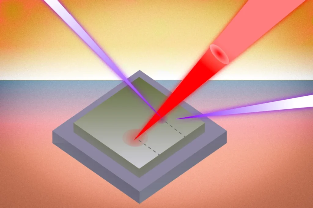
- Laser Pulses: Precisely timed laser pulses are used to locally heat the sample. As the laser introduces heat, the X-ray beam simultaneously scans the material, capturing how this heat dissipates across space in real-time.
The combined effect offers an unprecedented view of heat transfer. The laser-powered electron pulse can detect minute changes in material strain at the atomic level, which are direct indicators of thermal expansion and contraction. Simultaneously, the penetrating X-rays provide diffraction patterns that reveal the atomic structure and how it changes as heat propagates through different layers and across interfaces. By integrating these measurements, researchers gain a much clearer and more comprehensive understanding of how a material conducts heat.
Chuliang Fu, an MIT postdoc and co-lead author, highlights the transformative aspect: "Using previous measurement techniques, in real devices, you couldn’t resolve what happens on one layer versus another, so you’d just measure the average. X-rays can clearly show how heat propagates across the interface through their diffraction." This ability to differentiate thermal behavior between individual layers and at their interfaces is a game-changer for understanding the complex thermal landscapes within modern microelectronics.
Unveiling Hidden Flaws: The Gallium Nitride Case Study
To demonstrate the power and precision of their new technique, the MIT team applied it to a test device composed of a layer of gallium nitride (GaN) grown on a silicon substrate. Gallium nitride is a wide-bandgap semiconductor material that has garnered significant attention for its potential in high-power, high-frequency electronics due to its excellent electrical properties and its promising ability to conduct heat efficiently. However, the thermal performance of GaN-on-silicon devices has historically been observed to degrade due to the formation of tiny defects during the manufacturing process.
Using their novel X-ray and laser method, the researchers conducted a detailed analysis of the GaN-on-silicon device. The results were striking:
- Dramatic Reduction in Heat Dissipation: The technique precisely measured a fourfold reduction in heat dissipation specifically across a micron-scale "wrinkle defect" present on the device. This meant that at this tiny imperfection, the material’s ability to transfer heat plummeted by an astonishing 75%.
- Anisotropic Heat Spread: Furthermore, the defect was found to cause heat to spread unevenly, moving more easily in one direction than in another. This anisotropic thermal conductivity at the defect site further complicates heat management strategies.
- Significant Overall Drop: Beyond the localized defect, the researchers observed an overall 25% drop in heat dissipation across the materials compared to an idealized scenario, indicating that even subtle imperfections can have a substantial cumulative impact.
These findings are particularly significant because, as Professor Li points out, "When people model heat dissipation, they model perfect crystals without defects. But these types of large wrinkle defects are very common in 2D materials. People never even knew how much heat is blocked by these wrinkles. Those are things we can now directly observe with this technique." This ability to quantify the impact of real-world manufacturing imperfections, previously unaccounted for in theoretical models, is crucial for bridging the gap between ideal material properties and actual device performance.
Broader Implications and Future Trajectories
The implications of this MIT breakthrough extend far beyond academic curiosity, promising to profoundly influence the design and development of future electronic systems across various sectors:
- Semiconductor Industry Advancement: The ability to precisely diagnose thermal bottlenecks at the micro- and nanometer scale is exactly what the semiconductor industry has been "longing for," according to Professor Kim. A leading semiconductor industry consortium has already reportedly expressed interest in collaborating with the MIT team to apply this measurement technique to study different types of chips. This indicates the immediate practical value and industry readiness to adopt such a powerful diagnostic tool.
- Optimizing AI and High-Performance Computing: The burgeoning fields of AI and high-performance computing rely on increasingly powerful processors that generate immense heat. By enabling better thermal design, this technique will help develop more power-dense and efficient chips, accelerating the capabilities of AI models and supercomputers without succumbing to thermal limits.
- Advancing Flexible Electronics and Wearables: Flexible electronics and wearable devices demand compact, lightweight designs where every micron counts. Efficient heat management is critical for performance and user comfort. This technique will allow engineers to optimize material choices and geometries for these next-generation form factors.
- Enhancing Clean Energy Systems: From power converters in electric vehicles to solar cell arrays, efficient thermal management is crucial for the performance, reliability, and lifespan of clean energy technologies. The MIT method can help in designing more robust power electronics that can handle higher thermal loads, contributing to more sustainable energy solutions.
- From Diagnosis to Prevention: The research represents a crucial step beyond merely identifying hotspots. By understanding "heat carriers" – the phonons or electrons responsible for transporting thermal energy – and their interactions with defects, researchers can delve into the fundamental causes of thermal failure. This deeper insight will enable the proactive design of materials and device architectures that inherently resist overheating and localized hotspots, leading to more resilient and efficient products.
- Bridging Theory and Experiment: The technique provides direct experimental measurements that can validate or refine theoretical models of heat flow, particularly in complex geometries and heterogeneous materials. This iterative feedback loop between experiment and theory will accelerate the development of new materials and designs.
The team believes this approach is versatile and applicable to a wide array of materials and device types, offering a universal diagnostic platform for thermal challenges. "This will enable better thermal design of electronic systems," Kim asserts. "Even with the same type of materials, the geometry and how the materials are laid out is quite complicated, so it will show us how those differences impact thermal flow by providing direct experimental measurements."
The development of this pioneering technique underscores a critical juncture in the evolution of electronics. As the physical limits of traditional scaling are approached, innovations in materials science and thermal management become increasingly vital. The MIT team’s work offers a powerful lens through which to examine these challenges, promising to unlock new avenues for designing faster, more reliable, and more energy-efficient technologies that will shape the future of computing and beyond.
This significant research was made possible through the generous support of the U.S. Department of Energy, the U.S. National Science Foundation, and the MIT School of Engineering Distinguished Energy Efficiency Fellowship.
The full team of researchers contributing to this groundbreaking paper includes co-lead authors Thanh Nguyen PhD ’24 and MIT postdoc Chuliang Fu; PhD candidate Mouyang Cheng; Abhijatmedhi Chotrattanapituk ’21, SM ’26; Denisse Córdova Carrizales SM ’26; Eunbi Rha SM ’26; Tyra Espedal ’26; Buxuan Li PhD ’24; Shivam Kajale SM ’23, PhD ’26; Tongtong Liu PhD ’23; Kuan Qiao PhD ’22; University of Texas at Austin Assistant Professor Zhantao Chen SM ’18, PhD ’22; Argonne National Laboratory researchers Kumar Neeraj, Donald Walko, and Haidan Wen; MIT Principal Research Scientist Svetlana Boriskina; MIT Associate Professor Deblina Sarkar; and co-corresponding authors MIT Associate Professor Mingda Li and MIT Associate Professor Jeehwan Kim.