In the intricate realm of quantum materials, the formation of electronic order rarely adheres to a simple, uniform blueprint. Instead, it frequently manifests as highly complex, spatially heterogeneous patterns. Among the most fundamental and extensively studied examples of this phenomenon is the charge density wave (CDW), a collective electronic state where electrons organize into a periodic, repeating lattice structure, typically emerging at cryogenic temperatures. While charge density waves have been a focal point of condensed matter physics for decades, a significant challenge has persisted: the inability to directly observe, with spatial resolution, how their strength and spatial coherence evolve during a phase transition – the critical juncture where a material shifts from one state to another. This observational gap has long hampered a comprehensive understanding of these crucial electronic phases.
A groundbreaking achievement, poised to redefine our understanding of these quantum phenomena, has now been realized by a distinguished research team. Led by Professor Yongsoo Yang of the Department of Physics at the Korea Advanced Institute of Science and Technology (KAIST), and involving collaborations with Professors SungBin Lee, Heejun Yang, and Yeongkwan Kim, alongside colleagues at Stanford University, the team has, for the first time, directly visualized the evolution of charge density wave order’s amplitude across space within a quantum material. This unprecedented insight moves beyond indirect inferences, offering a direct window into the dynamic and often fragmented nature of electronic pattern formation.
The Breakthrough: Direct Visualization of CDW Evolution
The core of this scientific advancement lies in the team’s ability to precisely map the amplitude of charge density wave order as it forms, strengthens, weakens, and ultimately breaks apart across varying temperatures. This direct observation challenges long-held assumptions about the uniformity of phase transitions in quantum systems. Previously, experimental techniques provided only an averaged, bulk understanding of CDW behavior, or offered surface-sensitive insights. The KAIST-Stanford collaboration has pierced through this limitation, delivering spatially resolved data that reveals the microscopic intricacies of these electron organizations.
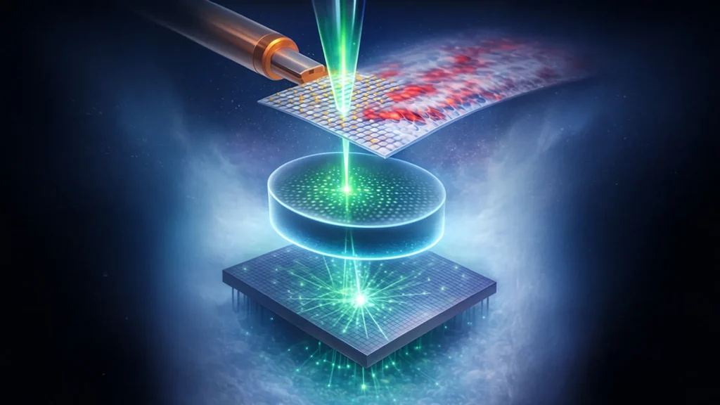
Their methodology employed a sophisticated experimental setup: a liquid-helium-cooled electron microscope integrated with four-dimensional scanning transmission electron microscopy (4D-STEM). This advanced configuration proved instrumental in overcoming the technical hurdles that had previously prevented such direct visualization. By operating at temperatures near absolute zero (approximately -253°C), the researchers could stabilize the delicate quantum states and capture the subtle electronic rearrangements. The nanoscale mapping capabilities of their system allowed them to not only ascertain the presence of electronic order but also to quantify its local strength and delineate how it connects or disconnects across different regions of the material.
Technological Innovation: The Power of 4D-STEM at Cryogenic Temperatures
The success of this research is inextricably linked to the innovative application of 4D-STEM under extreme cryogenic conditions. Traditional methods for probing charge density waves, such as X-ray diffraction or scanning tunneling microscopy (STM), each have inherent limitations. Diffraction techniques provide an averaged, reciprocal-space view of the periodic order across a macroscopic sample, obscuring local variations. STM, while offering atomic resolution, is primarily surface-sensitive and often cannot penetrate into the bulk of the material to reveal strain-induced effects or deep-seated inhomogeneities.
The 4D-STEM technique, however, captures a vast amount of information from the scattered electron beam at each probe position, effectively recording a full diffraction pattern for every point scanned across the sample. When combined with liquid helium cooling, this allows for the direct measurement of local electronic order with exceptional spatial resolution, down to structures as minute as one hundred-thousandth the width of a human hair. This capability is akin to observing ice crystals forming on a pond, but at an unimaginably high magnification and for electrons rather than water molecules. The extreme cold is crucial for stabilizing the fragile quantum phases, preventing thermal fluctuations from disrupting the ordered electronic states. This fusion of ultra-high-resolution imaging with precise temperature control represents a significant leap forward in experimental quantum materials science, providing a powerful new tool for exploring complex electronic landscapes.
Unveiling Patchy Electron Patterns: A New Paradigm
One of the most striking revelations from this study is the decidedly non-uniform manner in which electronic order manifests. Contrary to simplistic models that might envision a smooth, widespread formation of CDWs, the high-resolution images presented a picture of scattered, heterogeneous patterns. Some regions of the material exhibited clear, well-defined CDW patterns, signifying strong electronic order, while immediately adjacent areas showed no such order whatsoever. This observation fundamentally alters our understanding of how collective electronic states nucleate and propagate.
Professor Yang likened this phenomenon to a lake where ice forms in scattered patches rather than covering the entire surface uniformly. This "patchy" nature implies that the factors governing the formation and stability of CDWs are highly localized and sensitive to the microscopic environment within the crystal. This spatial inhomogeneity is not merely an aesthetic detail; it has profound implications for how these materials conduct electricity, interact with light, and potentially host other exotic quantum phenomena. Understanding the origins and dynamics of these patches is crucial for manipulating and harnessing the properties of quantum materials.
The Crucial Role of Strain: Microscopic Distortions, Macroscopic Effects
The study further uncovered a direct and potent link between these uneven electronic patterns and minute distortions within the crystal lattice. Even infinitesimal amounts of strain – local deformations in the crystal structure – far too subtle to be detected by conventional optical methods, were found to significantly weaken the amplitude of the charge density wave. This finding provides compelling, direct evidence that the seemingly innocuous lattice vibrations and structural imperfections play a pivotal role in shaping the electronic landscape of quantum materials.
The strong correlation between strain and electronic order highlights a critical interplay between structural and electronic degrees of freedom. In many quantum materials, the lattice is not merely a passive scaffold for electrons but an active participant in determining their collective behavior. This research underscores that even tiny, localized strains can act as "pinning centers" or disruptive forces, impeding the formation of coherent, long-range electronic order. This discovery opens new avenues for material design, suggesting that by precisely controlling or introducing specific strain patterns, scientists might be able to engineer desired electronic properties or stabilize novel quantum phases. For instance, creating areas of intentional strain could potentially create pathways or barriers for electronic transport, leading to new forms of quantum circuitry.
Persistent Pockets and Gradual Transitions: Beyond Simple Vanishing
Another surprising and highly significant result emerged regarding the phase transition itself. The researchers observed that small, isolated pockets of CDW order could persist even above the globally defined transition temperature, where long-range order is typically expected to vanish entirely. This discovery challenges the conventional view of phase transitions as sharp, uniform events where order disappears abruptly across the entire material.
Instead, the findings suggest a more nuanced, gradual process. Electronic order, rather than vanishing all at once, appears to lose its spatial coherence progressively. These lingering pockets indicate a competition between ordering forces and disordering thermal fluctuations, with local environments potentially stabilizing transient or metastable ordered regions. This phenomenon has profound implications for understanding the nature of phase transitions in complex systems, particularly those with strong electron-lattice coupling. It suggests that the transition is not a simple binary switch but a more intricate evolution involving the breakdown of long-range correlations while local order might endure in sheltered micro-regions.
Measuring How Electronic Order Fades: A New Metric
A key methodological achievement of this work is the first direct measurement of correlations in CDW amplitude. By analyzing how the strength of electronic order at one location relates to that at another, the researchers were able to quantitatively demonstrate how spatial coherence breaks down across the phase transition, even as local amplitude might persist. This level of granular detail was previously unattainable with traditional bulk diffraction measurements, which only provide an average correlation length, or with scanning probe techniques, which struggle with bulk information and cryogenic environments.
This ability to directly map and quantify amplitude correlations provides a powerful new metric for characterizing electronic phases and their transitions. It offers a crucial experimental handle on the concept of "local order" versus "long-range order," enabling physicists to distinguish between isolated, fluctuating ordered regions and genuinely coherent, macroscopic phases. This advancement is particularly critical for systems where quantum fluctuations or disorder play a significant role, blurring the lines between ordered and disordered states.
Broader Context: The Significance of Charge Density Waves
Charge density waves are far from being an isolated curiosity; they are a fundamental and ubiquitous feature in a wide array of quantum materials, including transition metal dichalcogenides, cuprate superconductors, and various rare-earth compounds. These collective electronic states often intertwine with other exotic phenomena, such as superconductivity, magnetism, and topological properties. Understanding the formation and evolution of CDWs is therefore not just an academic exercise but a critical step towards unraveling the mysteries of high-temperature superconductivity and developing novel electronic devices.
Historically, CDWs were first theoretically predicted in the 1930s and experimentally confirmed in the 1970s. Since then, research has primarily focused on their thermodynamic properties and average structural characteristics using techniques like X-ray diffraction and inelastic neutron scattering. While these methods provided invaluable insights into the existence and general properties of CDWs, they lacked the spatial resolution to capture the microscopic, heterogeneous details now revealed by the KAIST-Stanford team. This new experimental capability bridges a significant gap, allowing researchers to explore CDWs not just as abstract bulk properties but as dynamic, spatially varying electronic textures.
A New Framework for Understanding Quantum Materials and Their Implications
By directly mapping the spatial structure and correlations of charge density waves, this study introduces a new experimental framework for understanding how collective electronic order forms, evolves, and interacts within real quantum systems. This paradigm shift from indirect inference to direct visualization holds immense potential for accelerating discoveries in condensed matter physics and materials science.
The implications are far-reaching. For instance, in the quest for room-temperature superconductors, many theories involve the intricate interplay between CDWs and superconductivity. A deeper, spatially resolved understanding of CDW dynamics could unlock secrets to suppressing unwanted CDW formation that competes with superconductivity, or conversely, enhancing CDW-mediated superconductivity. Furthermore, the ability to observe the effects of strain at the nanoscale provides a pathway for engineers to intentionally introduce or mitigate strain in materials, thereby fine-tuning their electronic properties for applications in next-generation electronics, quantum computing, and spintronics. The insights gained could lead to the development of "strain-engineered" quantum devices, where local distortions are precisely controlled to create desired electronic pathways or quantum bits.
Official Statements and Acknowledgments
Professor Yongsoo Yang underscored the transformative nature of their findings: "Until now, the spatial coherence of charge density waves was largely inferred indirectly through bulk measurements. Our innovative approach allows us to directly visualize how electronic order varies across space and temperature, providing an unprecedented level of detail. More importantly, it enables us to identify the local factors, such as subtle strain fields, that either stabilize or suppress this order, fundamentally changing our perspective on these complex quantum phenomena."
The study, a testament to collaborative scientific endeavor, featured Seokjo Hong, Jaewhan Oh, and Jemin Park of KAIST as co-first authors, recognizing their significant contributions to the research. The seminal work was published in Physical Review Letters, a highly esteemed journal in the physics community, signifying its impact and novelty.
The research was primarily supported by substantial grants from the National Research Foundation of Korea (NRF) across various programs, including the Individual Basic Research Program, Basic Research Laboratory Program, and Nanomaterial Technology Development Program, funded by the Korean Government (MSIT). Additional financial support was provided by the KAIST singularity professor program for Professor Yang, NRF grants for Professors SungBin Lee, Yeongkwan Kim, and Heejun Yang, and the Korea Research Institute of Standards and Science (KRISS).
The sophisticated experimental work, specifically the 4D-STEM, ADF-STEM, and EELS experiments, was meticulously conducted using state-of-the-art equipment: a double Cs corrected Titan cubed G2 60-300 (FEI) and Spectra Ultra (ThermoFisher) at the KAIST Analysis Center for Research Advancement (KARA). The authors extended their gratitude to Hyung Bin Bae, Jin-Seok Choi, and the dedicated staff of KARA for their excellent technical support, which was indispensable to the success of this ambitious project. The team also acknowledged insightful discussions with E.-G. Moon, further highlighting the collaborative spirit that underpins significant scientific breakthroughs. This comprehensive and direct visualization capability marks a pivotal moment, offering a tangible path forward in the quest to harness the enigmatic properties of quantum materials for future technological advancements.