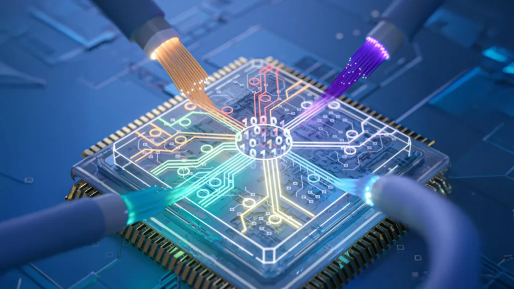
In a development that promises to redefine the boundaries of optical engineering and semiconductor manufacturing, researchers at the California Institute of Technology (Caltech) have pioneered a method to transport light across silicon wafers with unprecedented efficiency. By achieving signal loss levels at visible wavelengths that rival the performance of long-haul optical fibers, the team has cleared a significant hurdle in the development of next-generation photonic integrated circuits (PICs). This breakthrough, detailed in the journal Nature, offers a pathway toward ultra-coherent, energy-efficient systems that could revolutionize fields as diverse as artificial intelligence, quantum computing, and high-precision timekeeping.
For decades, the gold standard for light transmission has been the optical fiber—a strand of ultrapure glass capable of carrying data over thousands of kilometers with minimal degradation. While the telecommunications industry has successfully transitioned the world’s data onto these fibers, the challenge of replicating this "ultralow loss" performance on the scale of a microchip has remained elusive. Standard silicon-based chips, while excellent for electronics, typically suffer from significant light scattering and absorption, particularly when dealing with visible light. The Caltech team’s new platform, however, bridges this gap by bringing the material properties of high-end optical fiber directly onto the silicon wafers used in modern computer chip fabrication.
The Architecture of Ultralow Loss: Bringing Fiber to the Chip
The core of this innovation lies in the use of germano-silicate glass, the same high-purity material found in the core of optical fibers. Traditionally, photonic circuits on chips have relied on materials like silicon nitride or silicon-on-insulator. While these materials are effective for near-infrared light—the spectrum used in most current telecommunications—they struggle to maintain efficiency in the visible spectrum.
The Caltech researchers, led by Kerry Vahala, the Ted and Ginger Jenkins Professor of Information Science and Technology and Applied Physics, developed a technique to print germano-silicate waveguides onto standard 8-inch and 12-inch silicon wafers. Waveguides act as the "pipes" for light, guiding photons along specific paths on a chip. To maximize the utility of these pathways, the team arranged them in intricate spirals. This geometry allows light to travel an effective distance of several meters while being confined to a footprint only a few millimeters wide.
"For years, we have been working to translate the spool-based fabrication of optical fiber onto silicon wafers, while trying to preserve the fiber’s hallmark of ultralow loss," Professor Vahala explained. The shift toward fiber-like performance, particularly in the visible bands, is expected to enable a new class of technologies that rely on negligibly low circuit energy loss.
The Visible Spectrum Advantage: A 20-Fold Performance Leap
While the new germano-silicate platform matches the best-performing silicon nitride devices in the near-infrared range, its true superiority is revealed in the visible light spectrum. Visible light—spanning from violet to red—is essential for applications involving atomic transitions, such as those used in atomic clocks and quantum sensors.
One of the primary causes of signal loss in micro-scale waveguides is surface roughness. Even microscopic imperfections on the walls of a waveguide can cause light to scatter, much like how a rough mirror produces a blurry reflection. To combat this, the Caltech team utilized the relatively low melting temperature of germano-silicate to their advantage. By placing the fabricated devices into a furnace, they performed a "reflow" process. This thermal treatment allows the surface of the glass to soften and smooth out, reaching a level of smoothness that approaches the scale of individual atoms.
Hao-Jing Chen, a postdoctoral scholar and lead author of the study, noted that this reflow technique largely suppresses the severe scattering loss that has historically limited visible-light photonic circuits. "At visible wavelengths, our recent platform exceeds silicon nitride’s record by a factor of 20, and we have more room to improve," Chen stated.
The quantitative results of this improvement are staggering. In the world of lasers, loss is the enemy of coherence. Coherence refers to how long a laser can maintain a stable frequency. The Caltech team found that lasers integrated with their new platform showed a 100-fold improvement in coherence compared to previous chip-scale designs.
Bridging the Gap Between Large-Scale Infrastructure and Microchips
The practical implications of this research extend into the heart of the global digital infrastructure. As data centers grapple with the massive energy demands of artificial intelligence (AI) and cloud computing, the efficiency of data transfer has become a critical bottleneck.
Henry Blauvelt, Chief Technology Officer at Emcore and a visiting associate at Caltech, highlighted the importance of "interfacing." One of the greatest challenges in photonics is the "coupling loss" that occurs when light moves from a laser into a waveguide, or from a chip into an optical fiber. Because germano-silicate is the same material used in fibers, the transition of light between the chip and the external network is significantly more efficient.
"Germano-silicate waveguides demonstrate extremely low loss and are also readily adaptable to efficiently transfer light between optical fibers and semiconductor lasers," Blauvelt noted. Reducing these losses is of paramount importance for lowering the overall energy cost of server infrastructure, which currently accounts for a significant portion of global electricity consumption.
The Physics of the Ring Resonator: Why "Kilometer" Performance Matters on a Centimeter Chip
To the layperson, measuring signal loss over kilometers for a chip that is only two centimeters wide might seem counterintuitive. However, Kellan Colburn, a graduate student and co-lead author, explains that the "effective" distance traveled by light on a chip is often much longer than the physical dimensions of the device.
This is best illustrated by the "ring resonator," a fundamental component in photonics. A ring resonator captures light and forces it to circulate thousands or even millions of times within a tiny loop. Each time the light completes a lap, its intensity and phase interact with the light entering the ring. If the waveguide has high loss, the light fades quickly, and the resonator’s performance is poor. If the loss is ultralow, the light can travel the equivalent of several kilometers within the ring, leading to extremely high "Q-factors" (quality factors).
"That’s where low loss over meters, or ultimately kilometers, really matters," Colburn says. "The longer light can circulate, the higher the performance of resulting devices can be." For technologies like gyroscopes used in navigation or sensors used in medical diagnostics, this increased "circulation time" translates directly into higher sensitivity and accuracy.
Broad Applications: From Quantum Tech to Atomic Clocks
The versatility of the germano-silicate platform has led Professor Vahala to describe it as a "Swiss Army knife" for optics. By providing a low-loss environment across a wide range of wavelengths, the platform supports a variety of specialized applications:
- Atomic Clocks and Sensors: Many atomic operations—such as those involving the cooling and trapping of ions—require precise visible-light frequencies. Shrinking these systems from room-sized laboratory setups to chip-scale devices would allow for portable, ultra-precise timekeeping and navigation systems that do not rely on GPS.
- Quantum Computing: Quantum processors often use photons to carry information between qubits. Any loss of light results in a loss of quantum information. The ultralow-loss nature of this new platform could serve as the backbone for scalable quantum networks.
- AI and Data Centers: By reducing the heat generated by signal loss and improving the efficiency of laser sources, this technology could significantly reduce the carbon footprint of the massive data centers powering the AI revolution.
- Nonlinear Optics: The researchers also demonstrated nonlinear resonators capable of "frequency comb" generation. These devices can take a single color of laser light and turn it into a "rainbow" of precisely spaced frequencies, a tool used in everything from chemical sensing to exoplanet detection.
A Collaborative Global Effort
The research, titled "Towards fibre-like loss for photonic integration from violet to near-infrared," represents a multi-institutional effort. In addition to the core Caltech team, contributors included researchers from the University of California, Santa Barbara; Leiden University in the Netherlands; and the University of Southampton in the United Kingdom.
The project received significant backing from several high-level agencies, including the Defense Advanced Research Projects Agency (DARPA) and the Air Force Research Laboratory (AFRL). This support underscores the strategic importance of the technology, particularly for defense-related applications like secure communications and high-precision inertial navigation.
Future Outlook: The Path to Industrialization
While the current results are a landmark achievement, the Caltech team views this as a foundational step rather than a final product. The next phase of research will likely focus on further reducing the footprint of these devices and integrating them more deeply with active electronic components.
"We haven’t gone as far as we want to go, but we’ve made significant progress over the last five years," Vahala said. The ability to manufacture these circuits on 8- and 12-inch wafers is particularly promising, as these are the standard sizes used by commercial semiconductor foundries. This compatibility suggests that the transition from a laboratory breakthrough to mass-market industrial production may be shorter than is typical for such advanced materials science.
As the world increasingly relies on photons rather than electrons to move and process information, the ability to control light with the same precision and efficiency as a transcontinental fiber—but on the tip of a finger—marks a turning point in the silicon age. The "fiber-on-a-chip" is no longer a theoretical goal; it is a functioning reality poised to power the next century of technological innovation.